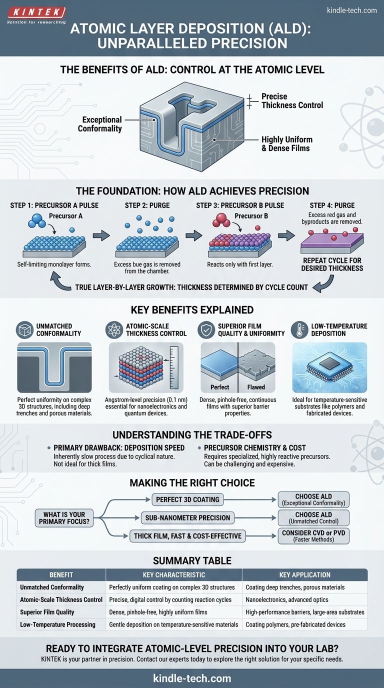
At its core, Atomic Layer Deposition (ALD) offers unparalleled control over the creation of ultra-thin films. Its primary benefits are exceptional conformality on complex surfaces, precise thickness control at the atomic level, and the ability to produce highly uniform and dense films. These advantages are a direct result of its unique, self-limiting, layer-by-layer growth mechanism.
Unlike traditional deposition methods that essentially 'spray' material onto a surface, ALD meticulously 'builds' a film one atomic layer at a time. This fundamental difference is the source of all its advantages, enabling the creation of flawless films on even the most complex 3D structures.
The Foundation: How ALD Achieves Precision
To understand the benefits of ALD, you must first understand its process. It is not a continuous deposition but a sequence of discrete, self-terminating steps.
The Self-Limiting Reaction
The process relies on sequential pulses of chemical precursors. A first gas precursor is introduced and forms a single, stable chemical layer (a monolayer) on the substrate. Critically, this reaction stops on its own once the entire surface is covered.
Any excess, unreacted gas is then purged from the chamber.
A second precursor is then introduced. It reacts only with the first layer, completing the deposition of a single, exceptionally thin layer of the final material. This cycle is then repeated to build the film.
True Layer-by-Layer Growth
Because each reaction cycle is self-limiting, it adds a predictable and fixed amount of material. The final film thickness is therefore determined simply by the number of cycles performed.
This removes the complexities of reactant flow rates and geometry that affect other deposition techniques, giving the engineer direct, digital control over the final thickness.
Key Benefits Explained
The unique ALD process directly translates into several powerful and distinct advantages over other thin-film deposition methods.
Unmatched Conformality
Because the process relies on gas-phase precursors that can diffuse into any exposed area, ALD can coat highly complex, three-dimensional structures with perfect uniformity.
This includes deep, narrow trenches and porous materials, achieving a consistent film thickness on all surfaces. This is a significant advantage over line-of-sight methods like sputtering.
Atomic-Scale Thickness Control
Since film growth is a direct function of counting reaction cycles, operators can achieve angstrom-level precision (one angstrom is one-tenth of a nanometer).
This level of control is essential for modern nanoelectronics, optics, and quantum devices where performance is dictated by dimensions at the atomic scale.
Superior Film Quality and Uniformity
The layer-by-layer process creates films that are incredibly dense, continuous, and free of pinholes. This results in superior barrier properties against moisture or chemical attack.
Furthermore, because the surface reactions are allowed to complete during each cycle, the film thickness is remarkably uniform across large-area substrates, such as 300mm silicon wafers.
Low-Temperature Deposition
ALD can often be performed at much lower temperatures than comparable methods like Chemical Vapor Deposition (CVD).
This makes it an ideal choice for depositing high-quality films on temperature-sensitive substrates, including polymers, plastics, and fully-fabricated electronic devices.
Understanding the Trade-offs
No technology is without its limitations. Objectivity requires acknowledging where ALD is not the best fit.
The Primary Drawback: Deposition Speed
The meticulous, cyclical nature of ALD makes it an inherently slow process. Purging the chamber between each precursor pulse takes time.
Building a film that is many nanometers thick can be time-consuming and costly compared to much faster bulk deposition methods.
Precursor Chemistry and Cost
ALD relies on pairs of highly reactive chemical precursors that exhibit the necessary self-limiting behavior. Developing or sourcing these specialized chemicals can be challenging and expensive.
Not all materials can be easily deposited with ALD because suitable precursors have not yet been identified or commercialized.
Making the Right Choice for Your Goal
Selecting ALD is a strategic decision based on whether your application demands its unique capabilities.
- If your primary focus is coating complex 3D nanostructures perfectly: ALD is likely the only viable method due to its exceptional conformality.
- If your primary focus is achieving sub-nanometer thickness precision: ALD's layer-by-layer control is unmatched and necessary for advanced electronics and optics.
- If your primary focus is depositing a thick film quickly and cost-effectively: You should consider alternative methods like CVD or PVD, as ALD's slow speed is a significant trade-off.
Ultimately, choosing ALD is a strategic decision to trade deposition speed for an unparalleled level of precision and perfection.
Summary Table:
| Benefit | Key Characteristic | Key Application |
|---|---|---|
| Unmatched Conformality | Perfectly uniform coating on complex 3D structures | Coating deep trenches, porous materials |
| Atomic-Scale Thickness Control | Precise, digital control by counting reaction cycles | Nanoelectronics, advanced optics |
| Superior Film Quality | Dense, pinhole-free, highly uniform films | High-performance barriers, large-area substrates |
| Low-Temperature Processing | Gentle deposition on temperature-sensitive materials | Coating polymers, pre-fabricated devices |
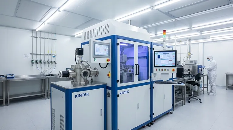
Ready to Integrate Atomic-Level Precision into Your Lab?
If your research or production demands flawless thin films with perfect conformality and atomic-scale control, KINTEK is your partner in precision. Our expertise in ALD technology and lab equipment can help you overcome the challenges of coating complex nanostructures and achieving the ultimate in film quality.
We specialize in providing solutions for laboratories that require:
- Perfect 3D Coating: Achieve uniform films on even the most intricate surfaces.
- Uncompromising Precision: Gain digital control over film thickness down to the angstrom level.
- Superior Material Performance: Develop dense, pinhole-free films for critical applications.
Let's discuss how ALD can advance your projects. Contact our experts today to explore the right solution for your specific needs.
Visual Guide
Related Products
- Cylindrical Resonator MPCVD Machine System Reactor for Microwave Plasma Chemical Vapor Deposition and Lab Diamond Growth
- Customer Made Versatile CVD Tube Furnace Chemical Vapor Deposition Chamber System Equipment
- 915MHz MPCVD Diamond Machine Microwave Plasma Chemical Vapor Deposition System Reactor
- Microwave Plasma Chemical Vapor Deposition MPCVD Machine System Reactor for Lab and Diamond Growth
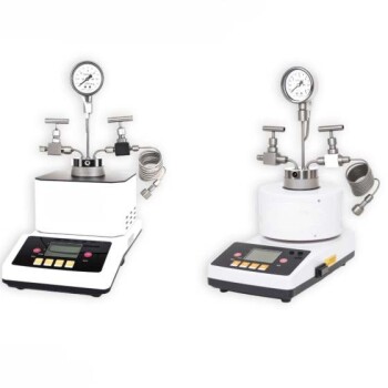
- Customizable Laboratory High Temperature High Pressure Reactors for Diverse Scientific Applications
People Also Ask
- What is MPCVD? Unlock Atom-by-Atom Precision for High-Purity Materials
- What pressure is needed for chemical vapor deposition of diamonds? Master the Low-Pressure 'Sweet Spot'
- How are CVD diamonds created? Discover the Science of Lab-Grown Diamond Precision
- What is the difference between MPCVD and HFCVD? Choose the Right CVD Method for Your Application
- What are the primary advantages of the CVD method for growing diamonds? Engineering High-Purity Gems and Components