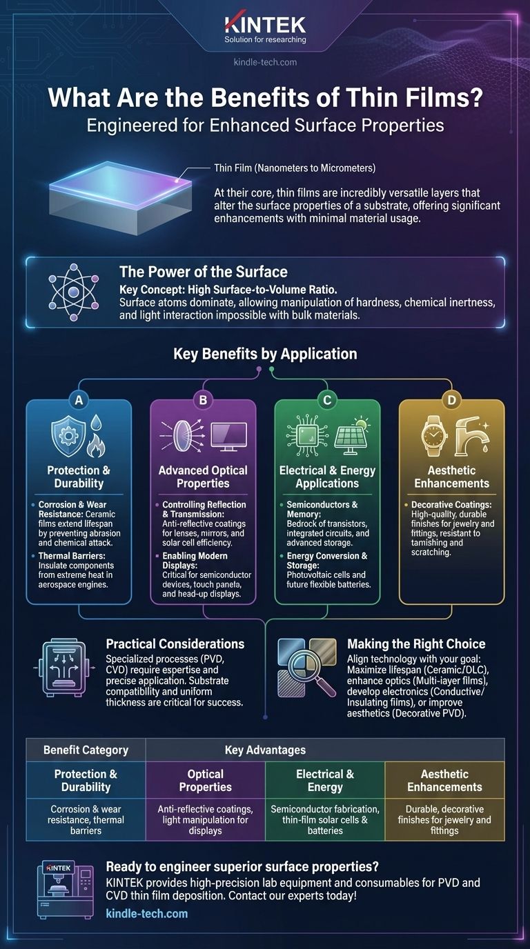
At their core, thin films are incredibly versatile layers of material, ranging from a few nanometers to several micrometers in thickness, engineered to alter the surface properties of a substrate. The primary benefits of applying a thin film include significantly enhancing a material's durability, providing powerful resistance to corrosion and wear, and creating specific optical or electrical properties that the base material does not possess.
The fundamental value of a thin film comes from its high surface-to-volume ratio. By reducing a material to an atomic scale, its properties change dramatically, allowing a tiny amount of specialized material to impart powerful new characteristics onto a much larger object.
The Foundation: Why Thin Films Are So Effective
Thin films are not simply a coat of paint; they are a fundamental re-engineering of a material's surface. This allows for a level of precision and performance that is impossible to achieve with the bulk material alone.
The Power of the Surface
The unique properties of thin films arise because at such small scales, the surface atoms dominate the material's behavior. This is a stark contrast to bulk materials, where the vast majority of atoms are on the interior.
This high surface-to-volume ratio is the key. It allows for the manipulation of properties like hardness, chemical inertness, and light interaction in ways the original material cannot.
Engineered for a Specific Purpose
Thin films are designed to perform a specific function. Whether protecting a jet engine turbine blade from heat or enabling a touch screen to function, the film is a targeted solution applied precisely where it is needed.
This targeted application makes them highly efficient, adding minimal weight or volume while delivering maximum impact.
Key Benefits by Application
The advantages of thin films are best understood by looking at their primary areas of use. They are broadly categorized by the type of problem they solve.
Category 1: Protection and Durability
This is one of the most common applications. Thin films act as a shield, protecting the underlying substrate from environmental damage.
Corrosion and Wear Resistance Ceramic thin films, for example, are exceptionally hard and chemically inert. When applied to cutting tools or industrial components, they can extend the equipment's lifespan by several orders of magnitude by preventing abrasion and chemical attack.
Thermal Barriers In high-temperature environments like aerospace engines, specialized thin films are used as thermal barriers. They insulate the underlying components from extreme heat, preventing failure and improving efficiency.
Category 2: Advanced Optical Properties
Thin films can manipulate light with incredible precision, making them essential for optics and displays.
Controlling Reflection and Transmission Multiple layers of thin films are applied to ophthalmic lenses to reduce glare (anti-reflective coatings). Conversely, they can be designed to create highly reflective surfaces for mirrors or to enhance the efficiency of solar cells by trapping more light.
Enabling Modern Displays Thin films are critical components in the production of semiconductor devices, touch panels, and head-up displays. Their specific electrical and optical properties are what allow these technologies to function.
Category 3: Electrical and Energy Applications
The unique electrical properties of thin films are the bedrock of the modern electronics industry.
Semiconductors and Memory The entire semiconductor industry is built upon the precise deposition of various thin films to create transistors and integrated circuits. They are also used to create advanced memory storage devices.
Energy Conversion and Storage Thin-film photovoltaic cells convert light directly into electricity. Similarly, ongoing research into thin-film batteries promises lighter, more flexible energy storage solutions for the future.
Category 4: Aesthetic Enhancements
Beyond pure function, thin films are also used for decorative purposes, providing a high-quality finish that is both beautiful and durable.
Decorative Coatings Thin films are used to apply attractive and resilient coatings to items like jewelry, watches, and bathroom fittings, providing colors and finishes that are resistant to tarnishing and scratching.
Understanding the Practical Considerations
While the benefits are significant, adopting thin film technology requires acknowledging its inherent complexities. It is not a universal solution, and its effectiveness depends entirely on proper engineering and application.
The Application Process is Specialized
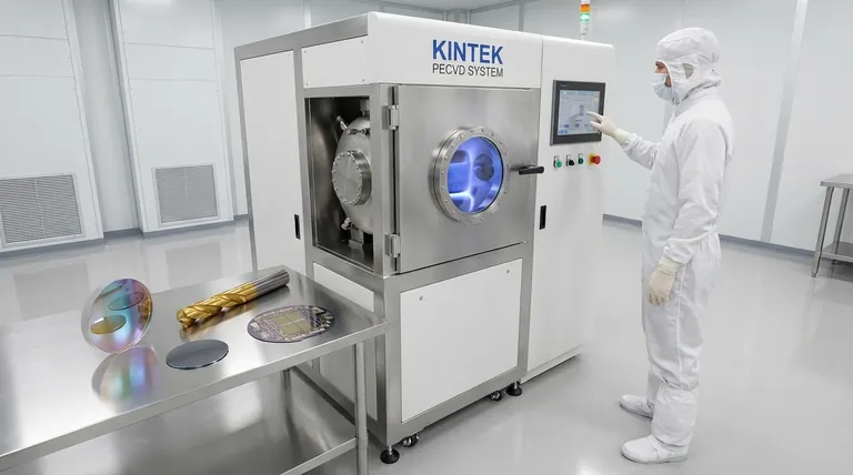
Applying a thin film is a highly technical process, often requiring a vacuum and sophisticated equipment for methods like physical vapor deposition (PVD) or chemical vapor deposition (CVD). This represents a significant investment in capital and expertise.
Substrate Compatibility is Critical
A film is only as good as its adhesion to the substrate. The choice of film material and deposition process must be carefully matched to the base material to ensure a strong, permanent bond. Poor adhesion can lead to delamination and complete failure of the coating.
Precision is Non-Negotiable
The properties of a thin film are directly tied to its thickness and uniformity. Even minor deviations can drastically alter its optical, electrical, or protective characteristics. Achieving this level of precision consistently is a major manufacturing challenge.
Making the Right Choice for Your Goal
To leverage thin films effectively, align your choice of technology with your primary objective.
- If your primary focus is maximizing lifespan and reliability: Prioritize hard, inert coatings like ceramic or diamond-like carbon (DLC) films for superior wear and corrosion resistance.
- If your primary focus is enhancing optical performance: Utilize multi-layer dielectric or metallic films designed specifically to control reflection, absorption, and transmission of light.
- If your primary focus is developing advanced electronics: The solution will involve a complex sequence of conductive, insulating, and semiconducting films tailored to build specific electronic components.
- If your primary focus is improving product aesthetics: Look to decorative PVD coatings that offer a wide range of durable colors and metallic finishes.
Ultimately, thin films empower you to bestow the ideal surface properties onto a material, creating a final product that is far greater than the sum of its parts.
Summary Table:
| Benefit Category | Key Advantages |
|---|---|
| Protection & Durability | Corrosion & wear resistance, thermal barriers |
| Optical Properties | Anti-reflective coatings, light manipulation for displays |
| Electrical & Energy | Semiconductor fabrication, thin-film solar cells & batteries |
| Aesthetic Enhancements | Durable, decorative finishes for jewelry and fittings |
Ready to engineer superior surface properties for your materials? KINTEK specializes in providing the high-precision lab equipment and consumables essential for thin film deposition processes like PVD and CVD. Whether you are developing advanced electronics, protective coatings, or optical components, our solutions help you achieve the precise, uniform thin films your research and production demand. Contact our experts today to discuss how we can support your laboratory's specific thin film application needs!
Visual Guide
Related Products
- Aluminized Ceramic Evaporation Boat for Thin Film Deposition
- Tungsten Evaporation Boat for Thin Film Deposition
- Electron Beam Evaporation Coating Oxygen-Free Copper Crucible and Evaporation Boat
- Molybdenum Tungsten Tantalum Evaporation Boat for High Temperature Applications
- HFCVD Machine System Equipment for Drawing Die Nano-Diamond Coating
People Also Ask
- What are thin films deposited by evaporation? A Guide to High-Purity Coating
- Why is an alumina boat selected for catalyst precursors? Ensure Sample Purity at 1000 °C
- What is the chemical method for thin film deposition? Build Films from the Molecular Level Up
- What is the widely used boat made of in thermal evaporation? Choosing the Right Material for High-Purity Deposition
- What are the applications of thin films deposition? Unlock New Possibilities for Your Materials


