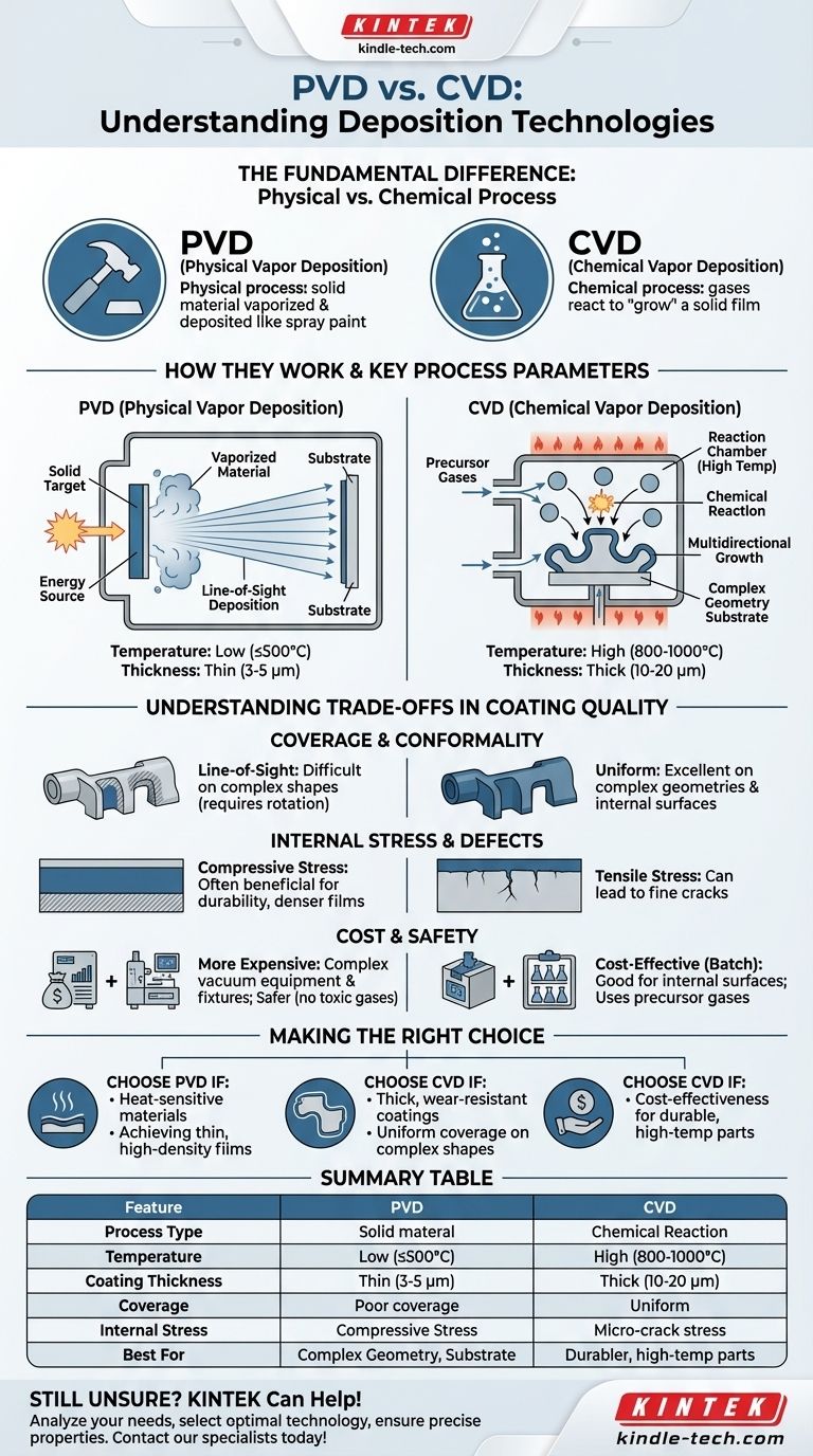
At its core, the difference is in the name. Physical Vapor Deposition (PVD) is a physical process where a solid material is vaporized and then deposited onto a substrate, much like spray painting on a microscopic level. In contrast, Chemical Vapor Deposition (CVD) is a chemical process where gases react inside a chamber to form a solid film that "grows" on the substrate surface.
The choice between PVD and CVD is a fundamental engineering trade-off. It forces a decision between PVD's lower-temperature precision for sensitive materials and CVD's high-temperature, comprehensive coverage for complex geometries.
The Fundamental Difference: Physical vs. Chemical Process
The most critical distinction lies in how the coating material arrives and forms on the part's surface. This single difference dictates nearly all other properties and limitations of the two methods.
How PVD Works: Line-of-Sight Deposition
In PVD, a solid target material is bombarded with energy (like a high-current arc) inside a vacuum chamber. This vaporizes the material into a plasma.
This vaporized material then travels in a straight line and condenses on the substrate, forming a thin, hard film. Because it's a line-of-sight process, any area not directly exposed to the source will not get coated.
How CVD Works: Chemical Reaction and Growth
CVD involves introducing one or more precursor gases into a high-temperature reaction chamber.
These gases decompose and react with each other and the substrate, forming a solid coating that builds up on all exposed surfaces. This is a multidirectional process, as the gases surround the part, allowing the film to grow uniformly even in complex areas.
Key Process Parameters Compared
The mechanics of each process lead to vastly different operating conditions, which in turn affect the final product and the materials you can work with.
Processing Temperature
CVD is a high-temperature process, typically operating between 800°C and 1000°C. This heat is necessary to drive the chemical reactions.
PVD is a low-temperature process by comparison, running at around 500°C or even lower. This makes it suitable for coating materials that cannot withstand the extreme heat of CVD.
Coating Thickness
CVD is generally used to create thicker coatings, often in the range of 10 to 20 micrometers (μm).
PVD produces thinner films, typically between 3 and 5 micrometers (μm). The resulting films are very dense and ultra-hard.
Understanding the Trade-offs in Coating Quality
Neither method is inherently superior; they simply offer different advantages and disadvantages based on the final application's requirements.
Coverage and Conformality
CVD provides excellent, uniform coverage on parts with complex geometries, including deep holes and internal walls. The gas-based process ensures the film grows everywhere.
PVD's line-of-sight nature makes it difficult to coat complex shapes uniformly. Parts often need to be rotated on complex fixtures to ensure adequate coverage, which adds cost and complexity.
Internal Stress and Defects
The high heat of CVD can cause tensile stress to build up in the coating as the part cools down. This stress can sometimes lead to the formation of fine cracks.
PVD's lower temperature process results in compressive stress, which is often beneficial for durability and performance. PVD coatings are also generally denser and have fewer voids than CVD coatings.
Cost and Safety
CVD is often more cost-effective for batch processing and is highly reliable for coating internal surfaces.
PVD can be more expensive due to the complex vacuum equipment and the intricate loading and fixing processes required. However, PVD avoids the toxic precursor gases often used in CVD, making it a safer process to handle.
Making the Right Choice for Your Application
Selecting the correct technology requires a clear understanding of your project's non-negotiable requirements, from the substrate material to the operating environment of the final part.
- If your primary focus is coating heat-sensitive materials or achieving a thin, high-density film: PVD is the superior choice due to its significantly lower processing temperatures.
- If your primary focus is achieving a thick, wear-resistant, and uniform coating on complex shapes with internal features: CVD is the clear winner because its chemical process coats all exposed surfaces evenly.
- If your primary focus is cost-effectiveness for durable parts that can withstand high temperatures: CVD often provides a more economical solution with excellent coating properties.
Understanding these core principles empowers you to select the right deposition technology not based on preference, but on the specific demands of your engineering challenge.
Summary Table:
| Feature | PVD (Physical Vapor Deposition) | CVD (Chemical Vapor Deposition) |
|---|---|---|
| Process Type | Physical (vaporization) | Chemical (gas reaction) |
| Temperature | Low (≤500°C) | High (800-1000°C) |
| Coating Thickness | Thin (3-5 μm) | Thick (10-20 μm) |
| Coverage | Line-of-sight (requires rotation) | Uniform (covers complex geometries) |
| Internal Stress | Compressive | Tensile |
| Best For | Heat-sensitive materials, thin dense films | Complex shapes, internal surfaces, batch processing |
Still Unsure Which Coating Technology is Right for Your Lab?
At KINTEK, we specialize in providing advanced lab equipment and consumables, including PVD and CVD systems tailored to your specific research and production needs. Our experts can help you:
- Analyze your substrate material and coating requirements
- Select the optimal deposition technology for your budget and goals
- Ensure you get the precise film properties your application demands
Let KINTEK empower your engineering challenges with the right coating solution. Contact our specialists today for a personalized consultation!
Visual Guide
Related Products
- Inclined Rotary Plasma Enhanced Chemical Vapor Deposition PECVD Equipment Tube Furnace Machine
- HFCVD Machine System Equipment for Drawing Die Nano-Diamond Coating
- 915MHz MPCVD Diamond Machine Microwave Plasma Chemical Vapor Deposition System Reactor
- Vacuum Hot Press Furnace Machine for Lamination and Heating
- Laboratory CVD Boron Doped Diamond Materials
People Also Ask
- What is plasma in CVD process? Lowering Deposition Temperatures for Heat-Sensitive Materials
- What is PECVD silicon deposition? Achieve Low-Temperature, High-Quality Thin Films
- What is the difference between PECVD and CVD? Unlock the Right Thin-Film Deposition Method
- How does plasma enhanced CVD work? Achieve Low-Temperature, High-Quality Thin Film Deposition
- What is the difference between CVD and PECVD? Choose the Right Thin-Film Deposition Method


