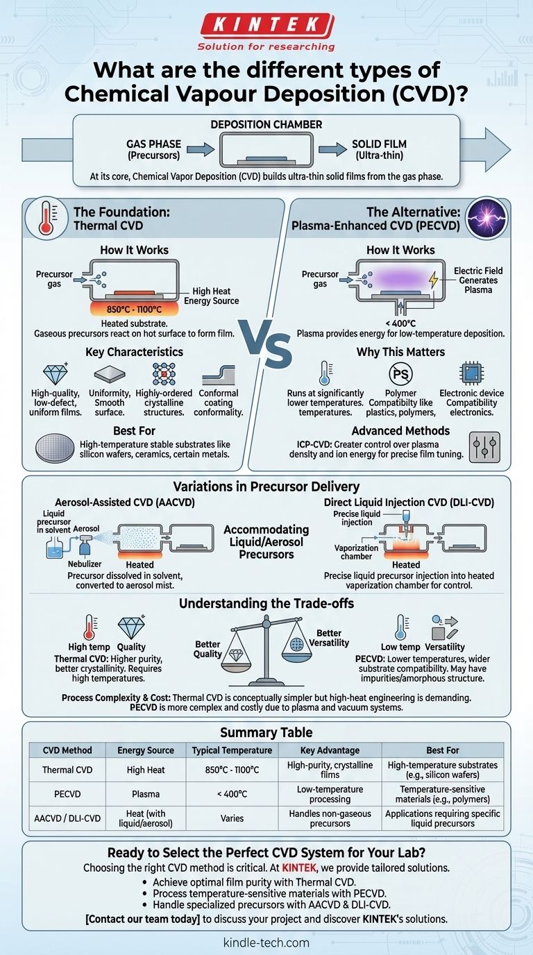
At its core, Chemical Vapor Deposition (CVD) is a process for building ultra-thin solid films from the gas phase. The different types of CVD are primarily distinguished by the energy source used to drive the chemical reaction—most commonly high heat (Thermal CVD) or an energy-rich plasma (Plasma-Enhanced CVD). Other variations focus on accommodating different chemical precursors, such as those delivered in a liquid or aerosol form.
The existence of different CVD methods boils down to a fundamental trade-off. You must choose between the high-quality films produced by high-temperature processes and the versatility of lower-temperature, plasma-assisted processes required for sensitive materials.
The Foundation: Thermal CVD
How It Works
Thermal CVD is the classic form of the process. A substrate is placed in a chamber and heated to a very high temperature, typically between 850°C and 1100°C. Gaseous chemical precursors are then introduced, which react or decompose on the hot surface to form a solid, thin film.
Key Characteristics
This method is renowned for producing high-quality films with low defect counts and excellent uniformity. Its ability to create highly-ordered crystalline structures makes it a leading approach for manufacturing advanced materials like graphene for high-performance electronics. The resulting films are also highly conformal, meaning they coat the underlying surface evenly, regardless of its topography.
The Alternative: Plasma-Enhanced CVD (PECVD)
The Role of Plasma
PECVD was developed to overcome the primary limitation of Thermal CVD: its extreme heat requirement. Instead of relying solely on temperature, PECVD uses an electric field to generate a plasma, an ionized gas containing highly energetic particles.
Why This Matters
This plasma provides the energy needed to break down the precursor gases and drive the deposition reaction. As a result, the process can run at significantly lower temperatures, often below 400°C. This makes PECVD essential for depositing films onto substrates that cannot withstand high heat, such as plastics, polymers, and fully assembled electronic devices.
Advanced Plasma Methods
More advanced techniques like Inductively Coupled Plasma CVD (ICP-CVD) offer even greater control over the plasma density and ion energy. This provides engineers with more precise tuning of the final film's properties.
Variations in Precursor Delivery
Aerosol-Assisted CVD (AACVD)
Some chemical precursors are not easily turned into a gas. AACVD solves this by dissolving the precursor in a solvent and generating a fine mist, or aerosol. This aerosol is then transported into the deposition chamber, where it vaporizes near the hot substrate to release the chemical for deposition.
Direct Liquid Injection CVD (DLI-CVD)
Similar to AACVD, DLI-CVD is designed for liquid precursors. In this method, a precise amount of the liquid precursor is injected into a heated vaporization chamber. This technique offers excellent control over the flow of material, which is critical for consistent and repeatable film growth.
Understanding the Trade-offs
Temperature vs. Film Quality
This is the most critical trade-off in CVD. The high temperatures of Thermal CVD generally produce films with higher purity and better crystallinity. Because PECVD operates at lower temperatures, its films can sometimes contain impurities (like hydrogen from precursor gases) or have a less ordered, amorphous structure.
Substrate Compatibility
The defining advantage of PECVD is its compatibility with a wide range of materials. The high heat of Thermal CVD severely restricts its use to substrates that are thermally stable, such as silicon wafers, ceramics, or certain metals.
Process Complexity and Cost
Thermal CVD systems are conceptually simpler, but the engineering required for safe, high-temperature operation is demanding. PECVD systems are more complex due to the need for plasma generation, vacuum systems, and radio-frequency (RF) power sources, which can increase equipment and operational costs.
Making the Right Choice for Your Goal
Selecting the correct CVD method requires a clear understanding of your primary objective.
- If your primary focus is the highest possible film purity and crystallinity: Start with Thermal CVD, assuming your substrate can tolerate temperatures often exceeding 800°C.
- If your primary focus is depositing films on temperature-sensitive materials (like polymers or completed electronics): PECVD is the essential choice, as it uses plasma to bypass the need for extreme heat.
- If your primary focus is using a specific liquid or low-volatility precursor: Investigate specialized systems like AACVD or DLI-CVD that are designed for non-gaseous chemical sources.
Understanding these core distinctions allows you to select the precise CVD method that aligns with your material, substrate, and performance requirements.
Summary Table:
| CVD Method | Energy Source | Typical Temperature | Key Advantage | Best For |
|---|---|---|---|---|
| Thermal CVD | High Heat | 850°C - 1100°C | High-purity, crystalline films | High-temperature substrates (e.g., silicon wafers) |
| PECVD | Plasma | < 400°C | Low-temperature processing | Temperature-sensitive materials (e.g., polymers) |
| AACVD / DLI-CVD | Heat (with liquid/aerosol precursor) | Varies | Handles non-gaseous precursors | Applications requiring specific liquid precursors |
Ready to Select the Perfect CVD System for Your Lab?
Choosing the right Chemical Vapor Deposition method is critical for achieving your desired film quality and substrate compatibility. At KINTEK, we specialize in providing tailored lab equipment solutions for all your deposition needs.
We help you:
- Achieve optimal film purity and crystallinity with our Thermal CVD systems
- Process temperature-sensitive materials efficiently with our Plasma-Enhanced CVD equipment
- Handle specialized precursors with our AACVD and DLI-CVD solutions
Our experts will work with you to identify the ideal CVD method for your specific application, materials, and performance requirements.
Contact our team today to discuss your project and discover how KINTEK's CVD solutions can advance your research and development.
Visual Guide
Related Products
- Chemical Vapor Deposition CVD Equipment System Chamber Slide PECVD Tube Furnace with Liquid Gasifier PECVD Machine
- RF PECVD System Radio Frequency Plasma-Enhanced Chemical Vapor Deposition RF PECVD
- Microwave Plasma Chemical Vapor Deposition MPCVD Machine System Reactor for Lab and Diamond Growth
- Customer Made Versatile CVD Tube Furnace Chemical Vapor Deposition Chamber System Equipment
- 915MHz MPCVD Diamond Machine Microwave Plasma Chemical Vapor Deposition System Reactor
People Also Ask
- What is plasma enhanced chemical vapor deposition PECVD equipment? A Guide to Low-Temperature Thin Film Deposition
- What are the core advantages of PE-CVD in OLED encapsulation? Protect Sensitive Layers with Low-Temp Film Deposition
- What types of substrates are used in CVD to facilitate graphene films? Optimize Graphene Growth with the Right Catalyst
- What are the processes of vapor phase deposition? Understand CVD vs. PVD for Superior Thin Films
- How are carbon nanotubes grown? Master Scalable Production with Chemical Vapor Deposition


