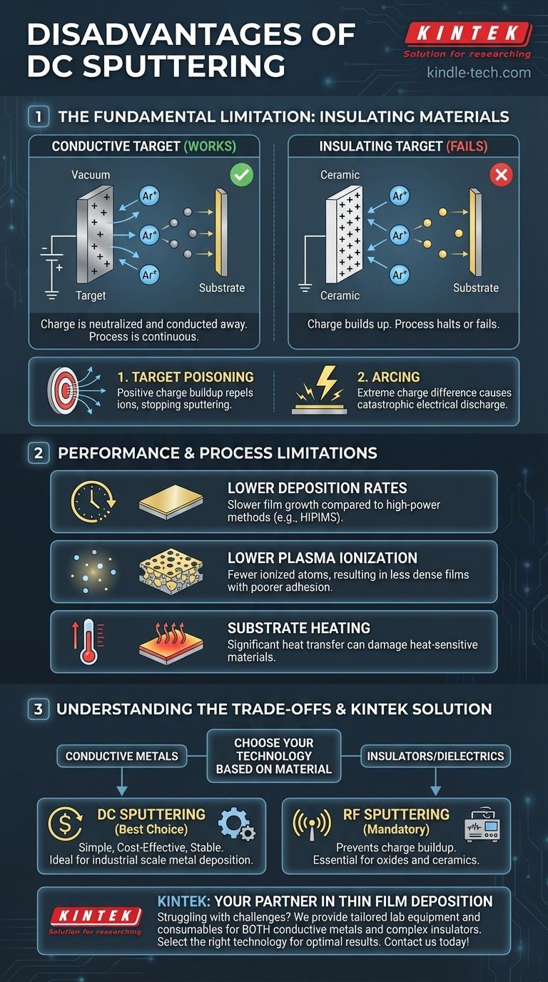
The primary disadvantage of DC sputtering is its fundamental inability to deposit non-conductive, or insulating, materials. This limitation stems from a process-halting phenomenon where electrical charge builds up on the surface of an insulating target. This can lead to destructive arcing or a complete stoppage of the sputtering process, rendering the technique ineffective for a wide range of common materials like oxides and ceramics.
While DC sputtering is a foundational and highly cost-effective method for depositing conductive metal films, its core limitation is a fundamental inability to process insulating materials. This forces a critical decision: leverage DC for its simplicity and low cost with metals, or adopt more complex technologies like RF sputtering for dielectrics.
The Fundamental Limitation: Insulating Materials
The core problem with DC (Direct Current) sputtering is tied directly to how the electrical circuit is completed within the vacuum chamber. This process works flawlessly for one class of materials but fails completely for another.
How DC Sputtering Works
In a standard DC sputtering setup, the target material is given a strong negative DC voltage. A process gas, typically argon, is introduced and ionized, creating a plasma. The positively charged argon ions are then accelerated toward the negatively charged target.
This bombardment physically ejects, or "sputters," atoms from the target material. These sputtered atoms then travel through the chamber and deposit as a thin film onto a substrate.
The Problem with Insulators
For this process to be continuous, the target must be electrically conductive. This allows the positive charge delivered by the argon ions to be neutralized and conducted away, maintaining the target's strong negative potential.
When the target is an insulating material (like a ceramic or oxide), it cannot conduct this charge away. Positive charge from the argon ions rapidly accumulates on the target's surface.
Consequence 1: Target Poisoning
As the insulating target becomes positively charged, it begins to electrostatically repel the incoming positive argon ions. This repulsion weakens and eventually stops the bombardment entirely. This effect is known as target poisoning, as the target surface becomes "poisoned" with a charge that halts the sputtering process.
Consequence 2: Arcing
If the charge buildup becomes extreme, the potential difference between the charged target and the grounded chamber components can become so great that it discharges catastrophically. This uncontrolled electrical discharge is known as arcing. Arcing can damage the target, contaminate the substrate, and create defects in the growing film.
Performance and Process Limitations
Beyond the primary issue with insulators, DC sputtering has other relative disadvantages when compared to more advanced techniques.
Lower Deposition Rates
Compared to high-power methods like HIPIMS (High Power Impulse Magnetron Sputtering), standard DC sputtering generally has a lower deposition rate. The process is less energetic, resulting in fewer atoms being ejected from the target per unit of time.
Lower Plasma Ionization
In DC sputtering, only a small fraction of the sputtered atoms become ionized themselves. More advanced techniques generate a much denser plasma, leading to a higher degree of ionization of the coating material. Higher ionization can result in denser, higher-quality films with better adhesion.
Substrate Heating
The energy transfer during sputtering can cause significant heating of the substrate. While this is an issue for many sputtering techniques, the lower efficiency of DC sputtering can sometimes exacerbate the problem for heat-sensitive substrates.
Understanding the Trade-offs: Cost vs. Capability
No technology exists in a vacuum. The disadvantages of DC sputtering are offset by significant, practical advantages that make it a dominant technique for specific applications.
The Advantage of Simplicity and Cost
DC sputtering is the simplest, most mature, and least expensive form of sputtering. DC power supplies are significantly cheaper and easier to implement than the complex RF (Radio Frequency) power supplies required for insulating materials. This makes it the go-to choice for depositing metals at industrial scale.
The Advantage of Stability (for Metals)
When used for its intended purpose—depositing conductive films—DC sputtering is exceptionally stable and easy to control. It allows for precise management of film thickness and uniformity over large areas.
The Clear Dividing Line
The choice between DC sputtering and an alternative is rarely ambiguous. If the target material is conductive, DC sputtering's cost and simplicity are major advantages. If the target is an insulator, DC sputtering is simply not a viable option, and a technique like RF sputtering becomes mandatory.
Making the Right Choice for Your Goal
Your choice of sputtering technology should be dictated entirely by your target material and performance requirements.
- If your primary focus is cost-effective deposition of a conductive metal: DC sputtering is almost always the correct choice due to its low equipment cost and process simplicity.
- If your primary focus is depositing a non-conductive or dielectric material (like an oxide or ceramic): You must use an alternative like RF sputtering to prevent the charge buildup that makes DC sputtering ineffective.
- If your primary focus is achieving the highest possible film density and adhesion on a complex surface: Consider more advanced techniques like HIPIMS, which overcomes the lower ionization efficiency of standard DC sputtering.
Understanding these fundamental trade-offs empowers you to select the most effective and economical deposition strategy for your specific application.
Summary Table:
| Disadvantage | Key Impact |
|---|---|
| Inability to Sputter Insulators | Process halts due to charge buildup; not suitable for ceramics or oxides |
| Lower Deposition Rates | Slower film growth compared to advanced methods like HIPIMS |
| Risk of Arcing and Target Poisoning | Can damage targets and contaminate substrates |
| Substrate Heating | May affect heat-sensitive materials |
| Lower Ionization Efficiency | Results in less dense films compared to high-ionization techniques |
Struggling with thin film deposition challenges? KINTEK specializes in lab equipment and consumables, providing tailored solutions for your sputtering needs. Whether you're working with conductive metals or complex insulators, our expertise ensures you select the right technology for optimal results. Contact us today to discuss how we can enhance your laboratory's capabilities and efficiency!
Visual Guide
Related Products
- Spark Plasma Sintering Furnace SPS Furnace
- Vacuum Induction Melting Spinning System Arc Melting Furnace
- Circulating Water Vacuum Pump for Laboratory and Industrial Use
People Also Ask
- Why are Spark Plasma Sintering (SPS) furnaces or hot presses utilized in the preparation of Li3PS4 solid electrolytes?
- What are the fundamentals of spark plasma sintering process? Unlock Rapid, High-Performance Material Consolidation
- What is the difference between spark plasma sintering and flash sintering? A Guide to Advanced Sintering Methods
- What is the pressure for spark plasma sintering? A Guide to Optimizing SPS Parameters
- What technical advantages does a Spark Plasma Sintering (SPS) furnace offer for LZP ceramics? Enhance Ionic Conductivity


