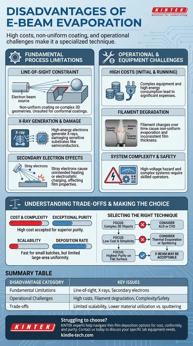
The primary disadvantages of e-beam evaporation are its high equipment and energy costs, its inability to uniformly coat complex, non-flat surfaces, and operational challenges like filament degradation that can affect process consistency. Because it is a line-of-sight deposition technique, it is fundamentally unsuited for applications requiring conformal coatings on intricate geometries.
While electron beam evaporation is a powerful tool for creating high-purity thin films, its significant drawbacks in cost, geometric limitation, and process control make it a specialized technique. Understanding these trade-offs is critical to determining if it is the right choice for your specific application.
Fundamental Process Limitations
The physics of how an electron beam generates vapor is the source of its most significant constraints. These are not flaws that can be easily engineered away but are inherent to the method itself.
The Line-of-Sight Constraint
E-beam evaporation is a "line-of-sight" process. Imagine trying to paint a complex sculpture using only a can of spray paint from a fixed position; you can only coat the surfaces you can directly see.
The vaporized material travels in a straight line from the source to the substrate. This makes it impossible to uniformly coat the inner surfaces of deep trenches, vials, or any other complex 3D geometry.
X-ray Generation and Substrate Damage
The high-energy electron beam does not just heat the source material. A side effect of bombarding a target with energetic electrons is the generation of X-rays.
These X-rays irradiate the substrate during deposition. For many standard optical coatings, this is not an issue, but it can cause significant damage to sensitive substrates, such as certain semiconductor devices or biological samples.
Secondary Electron Effects
Not all electrons are absorbed by the source material. Some are scattered or cause the emission of secondary electrons from the source.
These stray electrons can strike the substrate, leading to unintended heating or electrostatic charging. This can negatively impact film properties, adhesion, and the performance of electronic devices.
Operational and Equipment Challenges
Beyond the physics, the practical implementation of e-beam evaporation presents its own set of disadvantages related to cost, maintenance, and consistency.
High Initial and Running Costs
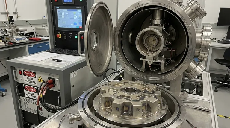
The equipment required for e-beam evaporation is complex and expensive. This includes high-voltage power supplies, powerful electron guns, and the associated high-vacuum systems.
Furthermore, the process is energy-intensive, leading to higher operational costs compared to simpler methods like thermal evaporation.
Filament Degradation and Inconsistency
The electron beam is generated by a heated tungsten filament. This filament degrades over time, slowly changing its properties.
This degradation can lead to instability in the electron beam, causing non-uniform evaporation rates. This directly harms the precision, uniformity, and reproducibility of your film thickness, a critical failure for many high-precision applications.
System Complexity and Safety
E-beam systems operate at very high voltages (typically several kilovolts), presenting a significant electrical safety hazard.
The overall system complexity demands highly skilled operators for routine use and maintenance, adding to the total cost of ownership.
Understanding the Trade-offs
No deposition technique is perfect. The disadvantages of e-beam must be weighed against its unique strengths, which are noted in some of the reference materials.
Cost and Complexity vs. Purity
The primary reason to accept the high cost and complexity of e-beam is to achieve exceptional film purity. The water-cooled copper crucible minimizes contamination from the container, a common problem in thermal evaporation where the boat material can co-deposit with the film.
Scalability vs. Deposition Rate
E-beam can achieve very high deposition rates (from 0.1 to over 100 µm/min), making it very fast for single-wafer or small-batch processing. However, achieving this rate uniformly over a large area is difficult and costly, which is why it is often considered to have limited scalability compared to methods like sputtering.
Material Utilization
Material utilization in e-beam is a nuanced issue. Compared to thermal evaporation, where material coats the entire chamber, e-beam is far more efficient. However, because the beam is focused on a small spot, it can "tunnel" into the source material, making it less efficient than sputtering, where the entire target surface is eroded more evenly.
Making the Right Choice for Your Application
Selecting a deposition method requires aligning the technique's capabilities with your project's most critical goal.
- If your primary focus is coating complex 3D objects: E-beam is unsuitable. You should consider a more conformal method like Atomic Layer Deposition (ALD) or Chemical Vapor Deposition (CVD).
- If your primary focus is low cost and operational simplicity: The high cost and complexity of e-beam make resistive thermal evaporation or DC sputtering more practical alternatives for many materials.
- If your primary focus is creating the highest-purity film from a wide range of materials on a flat surface: The disadvantages of e-beam are often an acceptable price for its superior purity and material versatility.
Understanding these inherent limitations is the first step toward selecting the optimal deposition technique for your specific engineering goal.
Summary Table:
| Disadvantage Category | Key Issues |
|---|---|
| Fundamental Limitations | Line-of-sight constraint, X-ray generation, secondary electron effects |
| Operational Challenges | High equipment/energy costs, filament degradation, system complexity/safety |
| Trade-offs | Limited scalability, lower material utilization vs. sputtering |
Struggling to choose the right deposition technique for your application?
At KINTEK, we specialize in helping laboratories navigate the complexities of thin-film deposition. Our experts can help you evaluate whether e-beam evaporation is the right choice or if an alternative like sputtering, thermal evaporation, or ALD would better suit your needs for cost, conformity, or purity.
Contact us today via our contact form to discuss your specific lab equipment and consumable requirements. Let KINTEK provide the precise solution you need to achieve your engineering goals.
Visual Guide
Related Products
- Electron Beam Evaporation Coating Oxygen-Free Copper Crucible and Evaporation Boat
- Electron Beam Evaporation Coating Tungsten Crucible and Molybdenum Crucible for High Temperature Applications
- Electron Beam Evaporation Coating Gold Plating Tungsten Molybdenum Crucible for Evaporation
- E Beam Crucibles Electron Gun Beam Crucible for Evaporation
- Electron Beam Evaporation Coating Conductive Boron Nitride Crucible BN Crucible
People Also Ask
- What is the temperature of e-beam evaporation? Mastering the Two-Zone Thermal Process for Precision Films
- How is an electron beam evaporator cooled during deposition? Essential Thermal Management for Stable Processes
- What is e-beam evaporation? Achieve High-Purity Thin Film Deposition for Your Lab
- What are the applications of electron beams? From Nanoscale Imaging to Industrial Manufacturing
- What are the applications of e-beam evaporation? Achieve High-Purity Coatings for Optics & Electronics


