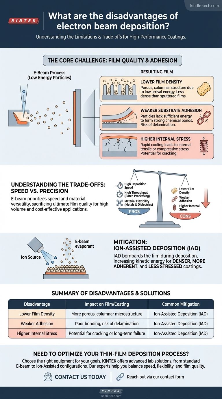
While powerful, electron beam (E-beam) deposition is not without its limitations. Its primary disadvantages stem from the relatively low energy of the evaporated particles, which can result in films that are less dense, have weaker adhesion to the substrate, and contain higher internal stress compared to films produced by other methods like sputtering. These are not universal flaws but rather inherent trade-offs for its high speed and material flexibility.
Electron beam deposition prioritizes deposition speed and material versatility over ultimate film quality. The core disadvantage is a potential reduction in film integrity—specifically lower density and weaker adhesion—which may require secondary processes like ion-assistance to overcome for demanding applications.
The Core Challenge: Film Quality and Adhesion
The fundamental physics of E-beam deposition, where a material is heated to its evaporation point in a vacuum, is the source of both its strengths and weaknesses. The evaporated atoms travel to the substrate with relatively low kinetic energy.
Lower Film Density
Because the depositing atoms or molecules arrive at the substrate surface with less energy, they have less mobility to arrange themselves into a tight, dense structure.
This can result in films that are more porous or columnar in their microstructure compared to the dense, glassy films often achieved with sputtering.
Weaker Substrate Adhesion
The low arrival energy of the evaporant also means the atoms do not impact the substrate with enough force to form the strongest possible bonds.
As a result, adhesion can be a significant concern. The reference to ion-assisted deposition, which increases "adhesion energy," directly highlights this inherent weakness in the standard E-beam process.
Potential for Internal Stress
The way films cool and solidify during E-beam deposition can lead to the buildup of internal tensile or compressive stress.
While ion-assisted deposition is noted to produce coatings with "less stress," this implies that unassisted E-beam films are more susceptible to this issue, which can cause cracking or delamination over time.
Understanding the Trade-offs: Speed vs. Precision
No deposition technique is perfect; choosing the right one involves understanding its trade-offs. E-beam excels in areas where other methods struggle, but this comes at a cost.
The Advantage of Speed and Volume
E-beam deposition is known for its high deposition rates, processing more rapidly in batch scenarios than methods like magnetron sputtering.
This speed makes it ideal for high-volume commercial applications where throughput is a critical economic factor.
The Benefit of Material Flexibility
E-beam technology can evaporate a very wide array of materials, including metals and dielectrics. The source materials are often less expensive than the specialized targets required for magnetron sputtering.
This flexibility and cost-effectiveness are major advantages for research and development or for coating with exotic materials.
When Disadvantages Become Dealbreakers
The lower density and weaker adhesion are not always problems. For simple optical coatings or decorative layers, these factors may be irrelevant.
However, for high-performance applications like semiconductor components, hard coatings for wear resistance, or medical implants, these disadvantages can be critical failures.
Mitigation: The Role of Ion-Assisted Deposition
The disadvantages of E-beam deposition are well-understood, and mature techniques exist to mitigate them. The most common is Ion-Assisted Deposition (IAD).
How Ion-Assist Works
In an IAD process, a separate ion beam bombards the substrate concurrently with the arrival of the evaporated material.
This bombardment transfers additional kinetic energy to the depositing atoms, effectively "hammering" them into a denser, more tightly-packed structure.
The Resulting Improvements
As noted in the references, this assistance results in "denser, more robust coatings" with significantly improved adhesion and lower internal stress.
IAD effectively buys back the film quality that is traded away for the speed and flexibility of the basic E-beam process, albeit with added complexity and cost.
Making the Right Choice for Your Application
Selecting a deposition method requires aligning the process capabilities with your project's final goal.
- If your primary focus is high-throughput and cost-efficiency: E-beam is an excellent choice, especially if ultimate film density and adhesion are not your top priorities.
- If your primary focus is maximum film density and durability: Standard E-beam may be insufficient, and you should consider either ion-assisted E-beam or an alternative method like magnetron sputtering.
- If your primary focus is material flexibility and rapid development: E-beam's ability to use a wide range of inexpensive evaporants makes it a highly flexible and powerful option.
Ultimately, understanding these trade-offs allows you to select E-beam deposition for its strengths while being fully prepared to mitigate its inherent weaknesses.
Summary Table:
| Disadvantage | Impact on Film/Coating | Common Mitigation |
|---|---|---|
| Lower Film Density | More porous, columnar microstructure | Ion-Assisted Deposition (IAD) |
| Weaker Adhesion | Poor bonding to substrate, risk of delamination | Ion-Assisted Deposition (IAD) |
| Higher Internal Stress | Potential for cracking or long-term failure | Ion-Assisted Deposition (IAD) |
Need to Optimize Your Thin-Film Deposition Process?
Choosing the right equipment is critical to achieving the desired film quality, whether you prioritize the high speed and material flexibility of E-beam deposition or require the superior density of sputtering. At KINTEK, we specialize in providing advanced lab equipment and consumables tailored to your specific laboratory needs. Our experts can help you select the perfect solution—from standard E-beam systems to ion-assisted configurations—to ensure your coatings meet the highest standards of performance and durability.
Contact us today to discuss your application and discover how KINTEK can enhance your research or production capabilities. Reach out via our contact form for a personalized consultation!
Visual Guide
Related Products
- Electron Beam Evaporation Coating Oxygen-Free Copper Crucible and Evaporation Boat
- Molybdenum Tungsten Tantalum Evaporation Boat for High Temperature Applications
- E Beam Crucibles Electron Gun Beam Crucible for Evaporation
- Electron Beam Evaporation Coating Tungsten Crucible and Molybdenum Crucible for High Temperature Applications
- Electron Beam Evaporation Coating Gold Plating Tungsten Molybdenum Crucible for Evaporation
People Also Ask
- What is e-beam evaporation? Achieve High-Purity Thin Film Deposition for Your Lab
- How is an electron beam evaporator cooled during deposition? Essential Thermal Management for Stable Processes
- What is the current of e-beam evaporation? A Guide to High-Purity Thin Film Deposition
- What is the container that holds the metal source material called in e-beam evaporation? Ensure Purity and Quality in Your Thin-Film Deposition
- What are the applications of e-beam evaporation? Achieve High-Purity Coatings for Optics & Electronics


