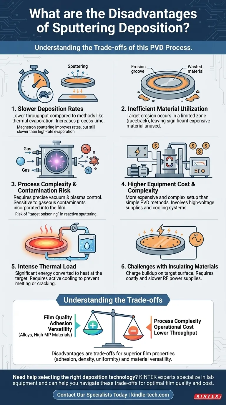
Sputtering deposition has several key disadvantages, including slower deposition rates compared to thermal evaporation, higher equipment complexity and cost, and challenges related to material utilization and process control. Gaseous contaminants can become trapped in the film, and the process generates significant heat at the target that must be managed.
While powerful and versatile, sputtering is not a universally superior technique. Its primary drawbacks center on process complexity, operational cost, and lower throughput, which represent a direct trade-off for its ability to produce high-quality, adhesive films from a vast range of materials.
Analyzing the Core Disadvantages
Sputtering is a physical vapor deposition (PVD) process prized for its control and the quality of the films it produces. However, these benefits come with inherent operational challenges that must be understood.
Deposition Rate and Material Efficiency
Sputtering is fundamentally a momentum-transfer process, which is inherently less efficient than boiling a material for thermal evaporation. This results in slower deposition rates, increasing process time and reducing throughput.
While techniques like magnetron sputtering significantly increase the rate by trapping electrons near the target, it often remains slower than high-rate evaporation methods.
Furthermore, sputtering makes inefficient use of the target material. The plasma is typically confined to a specific zone, leading to erosion in a "racetrack" pattern. A significant portion of the expensive target material is left unused.
Process Complexity and Contamination Risk
Sputtering requires a carefully controlled vacuum environment and a stable plasma. This introduces complexity and several points of potential failure.
The process involves bombarding a target with energetic ions (like Argon) inside a plasma. If trace amounts of reactive gases like oxygen or nitrogen are present in the chamber, the plasma can activate them, causing them to incorporate into the growing film as contaminants.
This is a particularly acute problem in reactive sputtering, where a gas is intentionally introduced to form a compound film. Precise control is needed to avoid "target poisoning," where the target surface becomes coated with the compound, drastically reducing the sputter rate.
Equipment Cost and Thermal Load
The equipment required for sputtering is generally more complex and expensive than for simpler PVD methods. It involves high-voltage power supplies (DC or RF), vacuum systems, gas flow controllers, and often, magnetic assemblies.
Depositing insulating materials is a major challenge, as charge builds up on the target surface. This requires using a more complex and costly Radio Frequency (RF) power supply, which also tends to have even lower deposition rates.
Finally, the majority of the energy from the bombarding ions is converted into heat at the target, not into ejecting atoms. This intense thermal load requires an active cooling system to prevent the target from melting, cracking, or degassing.
Understanding the Trade-offs
The disadvantages of sputtering should not be viewed in isolation but as trade-offs for its unique capabilities, especially when compared to a common alternative like thermal evaporation.
The Cost of Versatility
Sputtering's primary advantage is its ability to deposit almost any material, including alloys and refractory metals with extremely high melting points. Thermal evaporation struggles with these materials. Sputtering maintains the stoichiometry (elemental ratio) of the source target in the final film, which is critical for complex materials.
The Price of Film Quality
While the process can be slow and complex, sputtered films typically exhibit superior adhesion, higher density, and better uniformity over large areas compared to evaporated films. The energetic nature of the deposition process gives atoms mobility on the substrate surface, resulting in a denser, more robust film structure.
The Insulator Challenge
The difficulty and cost associated with sputtering insulators using RF power is a significant drawback. However, for many advanced optical and electronic applications, RF sputtering is one of the few viable methods for producing high-quality, dense oxide or nitride films.
Making the Right Choice for Your Application
Selecting a deposition method requires balancing your primary goal with the inherent costs and complexities of the process.
- If your primary focus is high throughput and low cost for simple metals: Thermal evaporation is often the more practical and economical choice.
- If your primary focus is film quality, adhesion, and material versatility: Sputtering is the superior technology for depositing dense films of alloys, compounds, or high-melting-point materials.
- If your primary focus is depositing high-quality insulating films: Be prepared for the higher cost, lower rates, and technical challenges of RF sputtering, but recognize it is a powerful and necessary tool for this task.
Ultimately, understanding these trade-offs allows you to choose sputtering deliberately for its strengths, while actively managing its inherent weaknesses.
Summary Table:
| Disadvantage | Key Challenge |
|---|---|
| Deposition Rate | Slower than thermal evaporation, reducing throughput. |
| Material Efficiency | Inefficient target use, leaving significant unused material. |
| Process Complexity | Requires stable plasma and vacuum, increasing risk of contamination. |
| Equipment Cost | More complex and expensive than simpler PVD methods. |
| Thermal Load | Generates significant heat, requiring active cooling systems. |
| Insulator Deposition | Requires costly RF power supplies and has lower rates. |
Need help selecting the right deposition technology for your lab?
Choosing between sputtering and other methods like thermal evaporation is a critical decision that impacts your project's cost, timeline, and final film quality. The experts at KINTEK specialize in lab equipment and consumables, and we can help you navigate these trade-offs.
We provide the guidance and equipment to ensure you achieve the film quality, adhesion, and material versatility you need, while managing complexity and cost. Let us help you optimize your thin-film processes.
Contact our specialists today for a personalized consultation!
Visual Guide
Related Products
- Chemical Vapor Deposition CVD Equipment System Chamber Slide PECVD Tube Furnace with Liquid Gasifier PECVD Machine
- Customer Made Versatile CVD Tube Furnace Chemical Vapor Deposition Chamber System Equipment
- HFCVD Machine System Equipment for Drawing Die Nano-Diamond Coating
- RF PECVD System Radio Frequency Plasma-Enhanced Chemical Vapor Deposition RF PECVD
- 915MHz MPCVD Diamond Machine Microwave Plasma Chemical Vapor Deposition System Reactor
People Also Ask
- What is plasma enhanced chemical vapor deposition PECVD equipment? A Guide to Low-Temperature Thin Film Deposition
- What are the core advantages of PE-CVD in OLED encapsulation? Protect Sensitive Layers with Low-Temp Film Deposition
- What happens during deposition chemistry? Building Thin Films from Gaseous Precursors
- What is the chemical vapor deposition growth process? Build Superior Thin Films from the Atom Up
- How are carbon nanotubes grown? Master Scalable Production with Chemical Vapor Deposition


