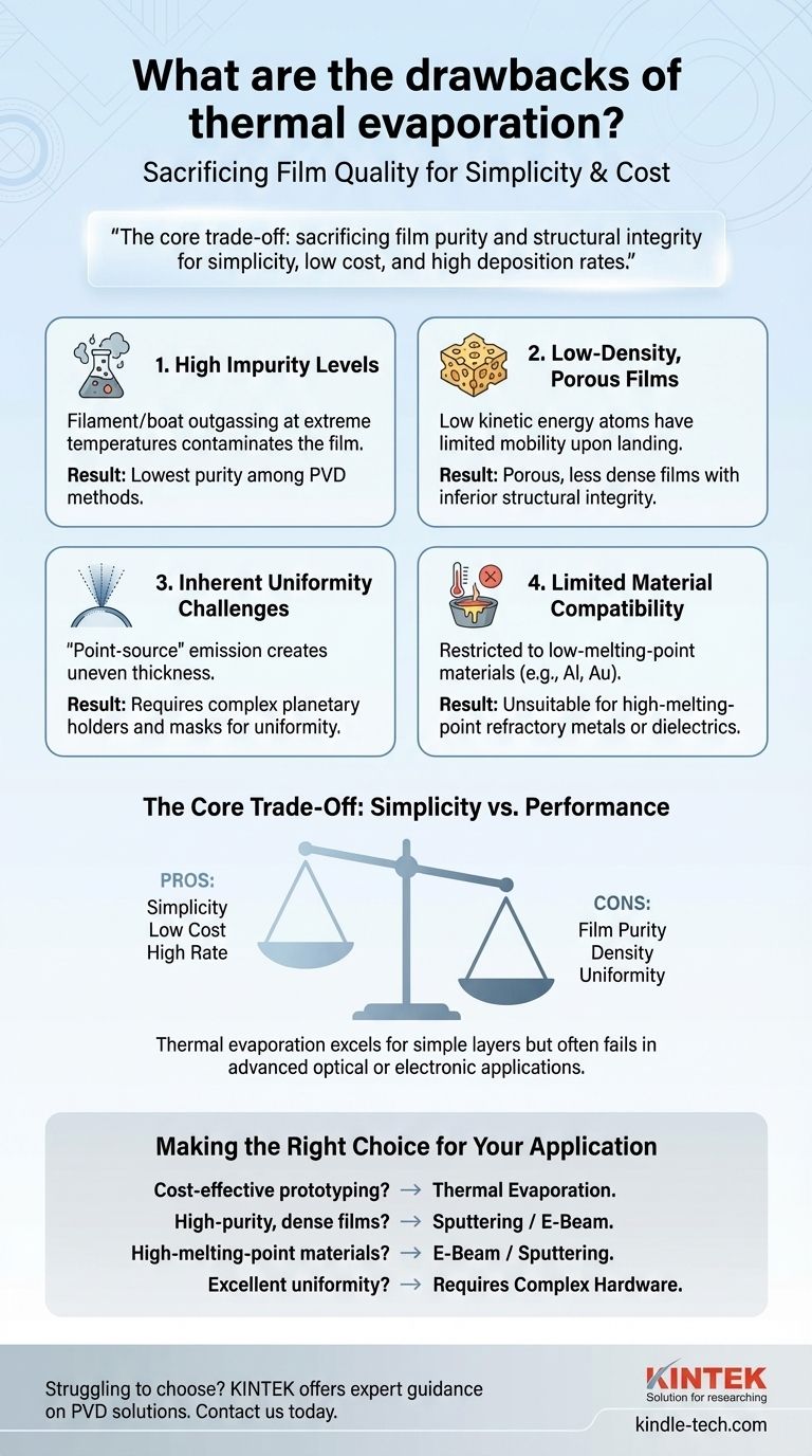
While a simple and cost-effective deposition technique, thermal evaporation has significant drawbacks that limit its use in high-performance applications. Its primary disadvantages are the introduction of high impurity levels, the creation of low-density films, poor thickness uniformity without specialized hardware, and a limited selection of materials it can effectively deposit. These issues stem directly from the method's reliance on resistively heating a source material to its vaporization point.
The core trade-off of thermal evaporation is sacrificing film purity and structural integrity for simplicity, low cost, and high deposition rates. While it excels in certain applications, its inherent limitations often make it unsuitable for advanced optical, electronic, or protective coatings where material quality is critical.
The Fundamental Limitations of Thermal Evaporation
To understand if thermal evaporation is right for your project, you must first grasp the technical reasons behind its drawbacks. These limitations are not equipment flaws but are inherent to the physics of the process.
High Impurity Levels
Resistive thermal evaporation often produces the least pure films among all Physical Vapor Deposition (PVD) methods. This is because the heating element—the filament or boat holding the source material—is heated to extreme temperatures, causing it to outgas impurities or even react with the material being evaporated.
This contrasts sharply with techniques like sputtering, where only the target material is bombarded, or E-beam evaporation, where an electron beam heats the source material directly, minimizing contact with other hot components.
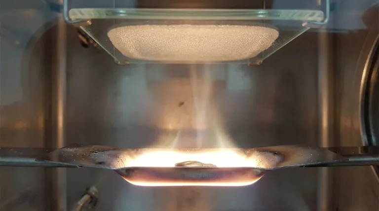
Low-Density and Porous Films
The atoms leaving the heated source in thermal evaporation have relatively low kinetic energy. When they arrive at the substrate, they have limited mobility to arrange themselves into a dense, tightly packed structure.
The result is often a film that is porous and has a lower density than the bulk material. While this can be partially improved with an ion-assist source to add energy to the depositing atoms, the films rarely match the density and quality achieved through more energetic processes like sputtering.
Inherent Uniformity Challenges
An evaporating source acts like a "point source," similar to a light bulb, emitting material in a plume. Without corrective measures, this results in a film that is thickest directly above the source and becomes progressively thinner toward the edges of the substrate.
Achieving good film uniformity requires complex and often expensive planetary substrate holders, which rotate and revolve the substrates through the vapor plume, along with precisely shaped uniformity masks to shield certain areas from deposition.
Limited Material Compatibility
The process is fundamentally limited by temperature. It is only suitable for materials with relatively low melting and boiling points, such as aluminum, gold, chromium, and various non-metals.
Materials that require extremely high temperatures to vaporize, such as refractory metals (tungsten, tantalum, molybdenum) or certain ceramic compounds, cannot be deposited with this method. They either fail to evaporate or require temperatures that would destroy the heating filament.
Understanding the Trade-offs: Simplicity vs. Performance
Despite its drawbacks, resistive thermal evaporation remains a widely used technique because its limitations are acceptable for many applications, especially when balanced against its significant advantages.
The Cost and Simplicity Advantage
Thermal evaporation systems are mechanically simpler and significantly less expensive than sputtering or E-beam systems. This makes them an ideal entry point for thin film research in university labs or for cost-sensitive industrial processes where ultimate film quality is not the primary driver.
The Rate and Directionality Benefit
For many metals, thermal evaporation offers a much higher deposition rate than sputtering. This speed is a major advantage in production environments. Furthermore, its "line-of-sight" directional deposition is highly effective for "lift-off" patterning, a common technique in microfabrication.
When Film Quality Is a Secondary Concern
Many applications do not require perfectly pure, dense films. For example, depositing a simple metallic layer for electrical contact, creating a reflective coating for a decorative part, or depositing indium bumps for wafer bonding are all excellent use cases for thermal evaporation.
The E-Beam Evaporation Distinction
It is critical to distinguish resistive thermal evaporation from Electron Beam (E-beam) evaporation. While both are "thermal" processes, E-beam uses a focused beam of electrons to heat the source material directly in its crucible. This technique overcomes the material temperature limitations and significantly reduces contamination from a heating element, allowing for higher purity films and the deposition of refractory metals and dielectrics.
Making the Right Choice for Your Application
Choosing the correct deposition method requires matching your application's needs to the process's capabilities.
- If your primary focus is cost-effective prototyping or simple metal layers: Resistive thermal evaporation is an excellent choice due to its low cost, simplicity, and high deposition rate.
- If your primary focus is high-purity, dense films for precision optics or electronics: The inherent impurity and density issues make thermal evaporation a poor fit; consider sputtering or E-beam evaporation instead.
- If you need to deposit high-melting-point materials or dielectric compounds: Resistive thermal evaporation is unsuitable; you must use E-beam evaporation or a sputtering technique.
- If you require excellent film uniformity over a large area: Thermal evaporation is only a viable option if your system is equipped with planetary substrate rotation and uniformity masks.
Ultimately, understanding these drawbacks allows you to leverage thermal evaporation for its strengths while avoiding its use in applications where film quality is non-negotiable.
Summary Table:
| Drawback | Description | Impact |
|---|---|---|
| High Impurity Levels | Heating element outgassing contaminates the film. | Reduces film purity, unsuitable for precision optics/electronics. |
| Low-Density, Porous Films | Low kinetic energy of deposited atoms limits packing. | Films are less durable and have inferior structural integrity. |
| Poor Thickness Uniformity | Point-source emission creates uneven deposition. | Requires complex planetary holders and masks for correction. |
| Limited Material Compatibility | Cannot effectively vaporize high-melting-point materials. | Restricts use to materials like Al, Au; not for refractory metals. |
Struggling to choose the right deposition technique for your lab's specific needs?
KINTEK specializes in lab equipment and consumables, offering expert guidance to help you select the perfect PVD solution—whether it's a cost-effective thermal evaporation system for prototyping or a high-performance sputtering or E-beam system for advanced applications. Our team can help you balance cost, simplicity, and film quality to achieve your project goals.
Contact us today via our [#ContactForm] to discuss your requirements and discover how KINTEK can enhance your laboratory's capabilities and efficiency.
Visual Guide
Related Products
- Molybdenum Tungsten Tantalum Evaporation Boat for High Temperature Applications
- Aluminized Ceramic Evaporation Boat for Thin Film Deposition
- Evaporation Boat for Organic Matter
- Electron Beam Evaporation Coating Tungsten Crucible and Molybdenum Crucible for High Temperature Applications
- High Purity Pure Graphite Crucible for Evaporation
People Also Ask
- What is the difference between thermal evaporation and e beam evaporation? Choose the Right Method for Your Thin Film
- What is the source of evaporation for thin film? Choosing Between Thermal and E-Beam Methods
- Is thermal evaporation used to deposit a thin metal film? A Guide to This Foundational PVD Technique
- What are thermal evaporation sources? Key Types and How to Choose the Right One
- What are the sources of thermal evaporation? A Guide to Resistive vs. E-Beam Heating