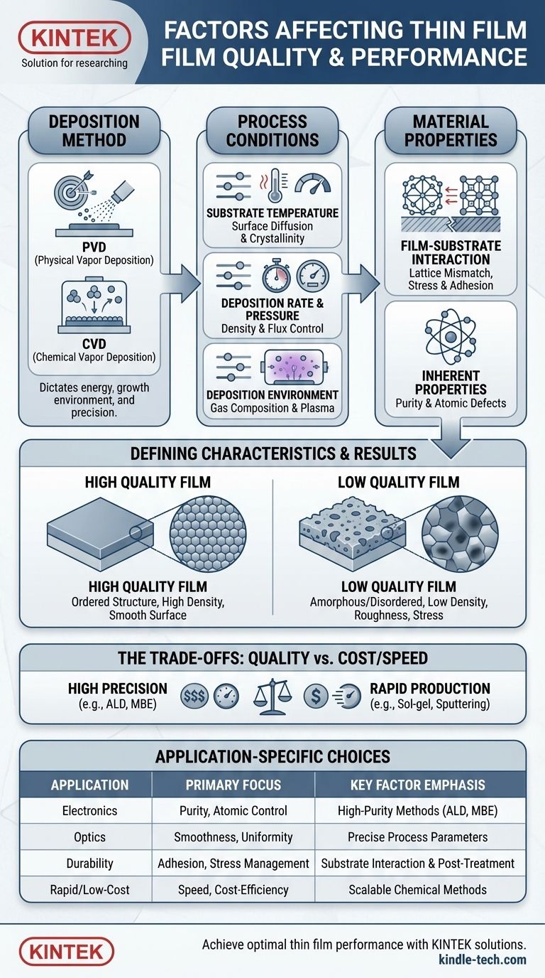
At its core, the quality and characteristics of a thin film are determined by three overarching categories of factors: the chosen deposition method, the specific conditions under which the film is grown, and the inherent properties of the materials being used. The final performance of any device relying on a thin film is a direct result of how these factors are managed and controlled during the manufacturing process.
The central takeaway is that a thin film is not simply a material; it is a complex structure whose final properties are an emergent result of the entire deposition process. Every decision, from the choice of deposition method to the substrate temperature, directly influences the film's atomic structure, internal stress, and ultimate performance.
The Foundation: Method and Materials
The first critical choices you make involve selecting the right deposition technique and understanding the interaction between your film and the surface it's grown on. These decisions set the fundamental constraints for the entire process.
The Choice of Deposition Technique
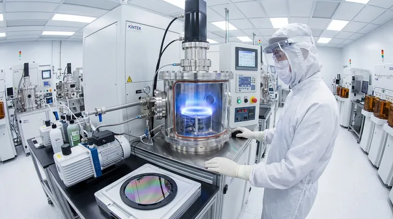
The method used to deposit the film is the most significant factor. Deposition techniques are broadly divided into two families: Physical Vapor Deposition (PVD) and Chemical Vapor Deposition (CVD).
PVD methods, like sputtering or thermal evaporation, physically transport material from a source to the substrate. Chemical methods, such as CVD, atomic layer deposition (ALD), or sol-gel, use chemical reactions on the substrate surface to form the film. This choice dictates the energy of arriving particles, the growth environment, and the achievable precision.
Substrate and Film Material Interaction
A thin film does not exist in isolation; it is grown on a substrate. Mismatches between the atomic lattice of the film and the substrate can create significant internal stress and strain.
This accumulated tension, if not managed, can lead to critical failures like cracking or delamination, where the film peels away from the substrate. The cleanliness and surface quality of the substrate itself are also paramount starting conditions.
Controlling the Growth: Critical Deposition Parameters
Once a method is chosen, the specific process variables must be precisely controlled. These parameters are the levers you pull to fine-tune the film’s final structure and properties.
Substrate Temperature
Temperature is a key variable that governs the mobility of atoms on the surface. Higher temperatures provide more energy for surface diffusion, allowing atoms to settle into more ordered, crystalline structures. Insufficient temperature can result in a more disordered, or amorphous, film.
Deposition Rate and Pressure
The speed at which material arrives at the substrate (flux) and the pressure inside the deposition chamber are critical. A very high deposition rate can "bury" defects before they have a chance to resolve, leading to a lower-density film. The chamber pressure affects how particles travel from the source to the substrate.
The Deposition Environment
The composition of the gas or plasma in the deposition chamber is fundamental. In CVD, the type and flow of precursor gases determine the film's chemical makeup. In PVD techniques like sputtering, the plasma environment—including the form of reactive ions (radicals) and their energy—directly influences the film's growth and chemistry.
The Result: Defining Film Characteristics
The interplay of deposition method and process parameters manifests in the film’s final physical and mechanical properties.
Grain Structure and Density
During growth, films form microscopic crystalline regions called grains. Irregular grain growth can create a "shadowing" effect, where some parts of the growing film are blocked by taller grains. This results in voids and a low-density film, which can compromise its mechanical and electrical integrity.
Surface Roughness and Imperfections
The final smoothness of the film is a direct outcome of the growth process. Surface roughness and other imperfections can dramatically impact performance, particularly in applications like optics, where they cause light scattering, or in electronics, where they can disrupt current flow.
Adsorption and Desorption Dynamics
At the atomic level, film growth is a balance between adsorption (atoms sticking to the surface) and desorption (atoms leaving the surface). The rates of these processes, influenced by temperature and pressure, determine the film's purity, density, and overall quality.
Understanding the Trade-offs: Failure Modes and Cost
Achieving a perfect thin film involves navigating a series of compromises and avoiding common pitfalls.
Internal Stress and Strain
As mentioned, stress is a primary failure mode. It arises not only from lattice mismatch but also from differences in thermal expansion between the film and substrate. Managing deposition settings and using post-deposition heat treatments (annealing) are key strategies to mitigate this risk.
Purity and Atomic-Scale Defects
For high-performance applications like semiconductors, purity is non-negotiable. Even a few misplaced atoms or impurities can catastrophically harm the performance of a microelectronic device. This necessitates high-precision deposition techniques and extremely clean manufacturing conditions.
Cost, Speed, and Precision
There is a constant trade-off between the quality of the film and the cost and efficiency of its production. Methods like Molecular Beam Epitaxy (MBE) or ALD offer unparalleled atomic-level control but are very slow and expensive. In contrast, techniques like dip coating or spin coating are fast and cheap but offer far less structural precision.
Making the Right Choice for Your Application
Your final selection of factors depends entirely on the intended use of the thin film.
- If your primary focus is high-performance electronics: Prioritize high-purity deposition methods like ALD or MBE that offer atomic-level control, accepting the higher cost and slower speed.
- If your primary focus is optical coatings: Meticulously control deposition parameters to minimize surface roughness and ensure uniform film density, as these directly impact optical properties.
- If your primary focus is mechanical durability: Concentrate on managing internal stress and promoting strong film-substrate adhesion to prevent cracking and delamination.
- If your primary focus is rapid or low-cost production: Consider scalable chemical methods like sol-gel or sputtering, while understanding and accepting the inherent trade-offs in film precision.
Ultimately, mastering thin film technology lies in understanding and controlling the direct relationship between your deposition process and the final film properties you need to achieve.
Summary Table:
| Factor Category | Key Elements | Impact on Film |
|---|---|---|
| Deposition Method | PVD (Sputtering), CVD, ALD | Determines particle energy, growth environment, and precision |
| Process Parameters | Substrate temperature, deposition rate, pressure | Controls film structure, density, and surface roughness |
| Material Properties | Film-substrate interaction, lattice mismatch | Influences internal stress, adhesion, and risk of delamination |
Achieve optimal thin film performance for your laboratory applications. The quality of your thin films directly impacts the success of your research and development. KINTEK specializes in providing high-quality lab equipment and consumables tailored to your deposition needs. Whether you require precise control for semiconductor fabrication, uniform coatings for optics, or durable films for mechanical applications, our expertise ensures you get reliable results. Contact us today to discuss how our solutions can enhance your thin film processes and drive your innovations forward.
Visual Guide
Related Products
- Aluminum-Plastic Flexible Packaging Film for Lithium Battery Packaging
- Thin-Layer Spectral Electrolysis Electrochemical Cell
People Also Ask
- How is aluminum foil utilized as a consumable during the assembly of cold sintering molds? Optimize Tooling Longevity
- How to tell if a lithium-ion battery is bad? Spot the critical signs of failure before it's too late.
- What is organic thin film? A Guide to Engineered Molecular Layers for Advanced Tech
- What are the properties of Aluminium (Al) relevant to its use in coatings? High Reflectivity & Conductivity Explored
- What are the three types of lamination? Choose the Perfect Finish for Your Print Project

