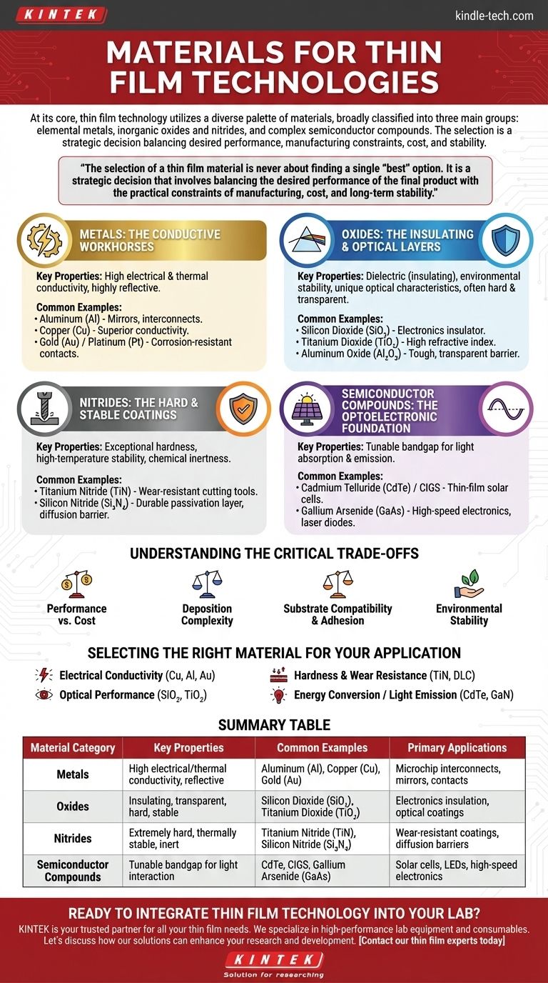
At its core, thin film technology utilizes a diverse palette of materials, which are broadly classified into three main groups: elemental metals, inorganic oxides and nitrides, and complex semiconductor compounds. The specific material is chosen based on the unique electrical, optical, or mechanical properties required for a given application, from microchips to solar panels.
The selection of a thin film material is never about finding a single "best" option. It is a strategic decision that involves balancing the desired performance of the final product with the practical constraints of manufacturing, cost, and long-term stability.
The Primary Material Categories Explained
Understanding the fundamental properties of each material family is the first step in designing a successful thin film application. Each category serves a distinct purpose, defined by its atomic structure and chemical composition.
Metals: The Conductive Workhorses
Metals are foundational materials in thin films, primarily valued for their excellent electrical and thermal conductivity. They are also often highly reflective.
Common examples include Aluminum (Al) for mirrors and interconnects in integrated circuits, Copper (Cu) for its superior conductivity in modern microchips, and Gold (Au) or Platinum (Pt) for corrosion-resistant electrical contacts.
Oxides: The Insulating and Optical Layers
Oxide films are prized for their dielectric (insulating) properties, environmental stability, and unique optical characteristics. Many are also very hard and transparent.
Silicon Dioxide (SiO₂) is the quintessential insulator in electronics. Titanium Dioxide (TiO₂) is used for its high refractive index in optical coatings, while Aluminum Oxide (Al₂O₃) provides a tough, transparent protective barrier.
Nitrides: The Hard and Stable Coatings
Nitrides are compounds known for their exceptional hardness, high-temperature stability, and chemical inertness. This makes them ideal for protective coatings in harsh environments.
Titanium Nitride (TiN) is famous for the gold-colored, wear-resistant coating on cutting tools and drills. Silicon Nitride (Si₃N₄) serves as a durable passivation layer and diffusion barrier in semiconductor manufacturing.
Semiconductor Compounds: The Optoelectronic Foundation
This diverse group of materials forms the basis of modern optoelectronics. Their defining feature is a tunable bandgap, which allows them to absorb and emit light at specific wavelengths.
Materials like Cadmium Telluride (CdTe) and Copper Indium Gallium Selenide (CIGS) are leading candidates for thin-film solar cells. Gallium Arsenide (GaAs) is used in high-speed electronics and laser diodes.
Understanding the Critical Trade-offs
The ideal material on paper may be impractical in reality. A successful design always accounts for the following trade-offs.
Performance vs. Cost
There is a constant balance between a material's ideal properties and its price. For example, gold is an excellent, non-oxidizing conductor, but copper and aluminum offer 90% of the performance for a fraction of the cost in most applications.
Deposition Complexity
Some materials are far more difficult to deposit than others. Simple metals can be easily evaporated or sputtered, but complex compounds like CIGS require precise control over multiple sources to achieve the correct chemical ratio (stoichiometry).
Substrate Compatibility and Adhesion
A thin film is useless if it does not adhere to the surface it is deposited on. Material choice is constrained by the substrate, as differences in thermal expansion can cause the film to crack or peel when heated or cooled.
Environmental Stability
The long-term reliability of a device depends on the film's stability. A material may have perfect initial properties but quickly degrade when exposed to oxygen, moisture, or high temperatures, requiring a protective "capping layer" of a more robust material.
Selecting the Right Material for Your Application
Your final choice depends entirely on your primary engineering goal.
- If your primary focus is electrical conductivity: Consider metals like copper or aluminum for general use, or gold for high-reliability, corrosion-proof contacts.
- If your primary focus is optical performance: Explore oxides like silicon dioxide for anti-reflection or titanium dioxide for high refractive index applications.
- If your primary focus is hardness and wear resistance: Focus on nitrides like titanium nitride or other hard coatings like diamond-like carbon (DLC).
- If your primary focus is energy conversion or light emission: Investigate semiconductor compounds like CdTe for solar cells or Gallium Nitride (GaN) for LEDs.
Mastering the interplay between these material families and their trade-offs is the key to engineering effective and reliable thin film devices.
Summary Table:
| Material Category | Key Properties | Common Examples | Primary Applications |
|---|---|---|---|
| Metals | High electrical/thermal conductivity, reflective | Aluminum (Al), Copper (Cu), Gold (Au) | Microchip interconnects, mirrors, contacts |
| Oxides | Insulating, transparent, hard, stable | Silicon Dioxide (SiO₂), Titanium Dioxide (TiO₂) | Electronics insulation, optical coatings |
| Nitrides | Extremely hard, thermally stable, inert | Titanium Nitride (TiN), Silicon Nitride (Si₃N₄) | Wear-resistant coatings, diffusion barriers |
| Semiconductor Compounds | Tunable bandgap for light interaction | CdTe, CIGS, Gallium Arsenide (GaAs) | Solar cells, LEDs, high-speed electronics |
Ready to Integrate Thin Film Technology into Your Lab?
Selecting the perfect material is just the first step. Achieving consistent, high-quality thin film deposition requires precise equipment and expert support.
KINTEK is your trusted partner for all your thin film needs. We specialize in providing high-performance lab equipment and consumables for deposition processes, helping researchers and engineers like you turn material science into real-world innovation.
We can help you:
- Identify the optimal deposition system for your specific material and application.
- Source high-purity targets and evaporation materials for reliable, repeatable results.
- Access expert technical support to optimize your process parameters.
Don't let equipment limitations hinder your project's potential. Let's discuss how our solutions can enhance your research and development.
Contact our thin film experts today for a personalized consultation!
Visual Guide