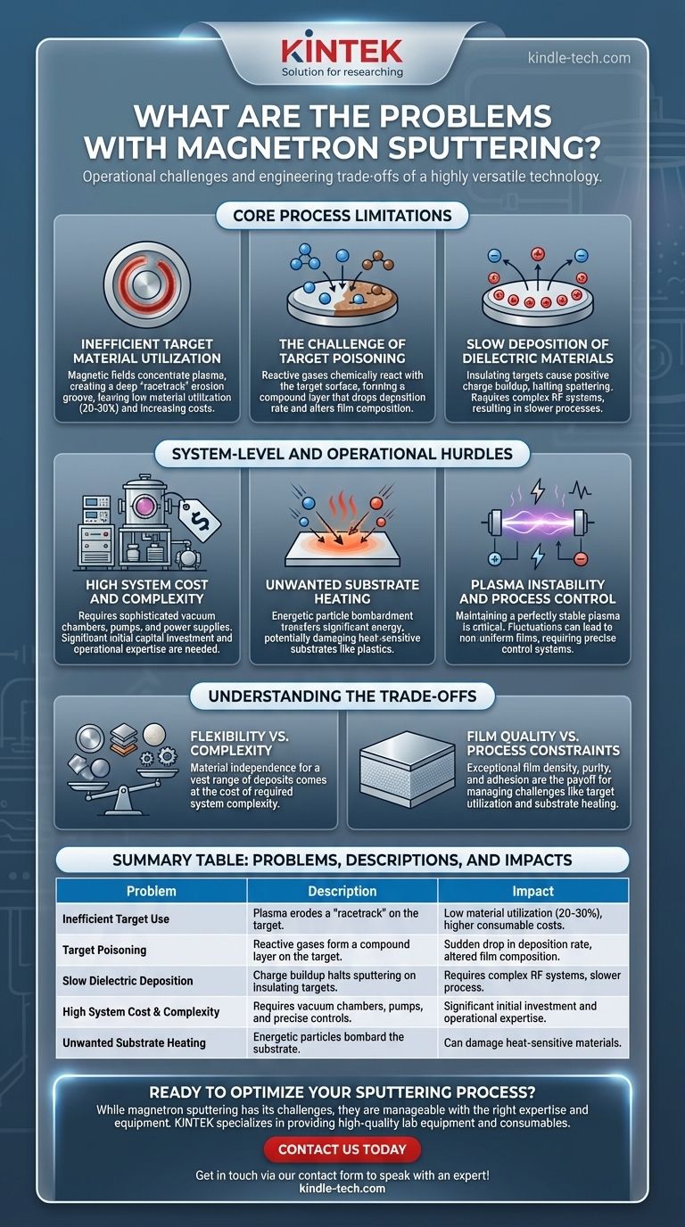
While a highly versatile technology, magnetron sputtering is not without its operational challenges. The primary problems include inefficient use of the target material, significant difficulty and slow deposition rates for dielectric (insulating) materials, the risk of "target poisoning" in reactive processes, and the high initial cost and complexity of the required vacuum systems.
The disadvantages of magnetron sputtering are not fundamental flaws but rather inherent engineering trade-offs for its exceptional flexibility and film quality. Understanding these limitations is the key to managing them effectively and deciding if it's the right process for a specific application.
Core Process Limitations
At its heart, magnetron sputtering relies on a carefully controlled plasma within a vacuum. The physics of this process gives rise to several key challenges that must be managed.
Inefficient Target Material Utilization
The magnetic fields used to confine the plasma and increase sputtering efficiency also cause it to concentrate in a specific area on the target surface.
This creates a deeper erosion groove, often called a "racetrack," leaving much of the target material unused. This low utilization rate, sometimes as low as 20-30%, increases the overall cost of consumables.
The Challenge of Target Poisoning
When sputtering in the presence of a reactive gas (like oxygen or nitrogen) to create compound films like oxides or nitrides, a phenomenon called target poisoning can occur.
The reactive gas can chemically react with the target surface itself, forming a layer of the compound material. This new layer often has a much lower sputter yield, causing a sudden drop in deposition rate and potentially altering the final film's chemical composition (stoichiometry).
Slow Deposition of Dielectric Materials
Magnetron sputtering is highly effective for conductive materials like metals. However, it is notoriously slow when depositing dielectrics (insulators).
This is because positive ion charge can build up on the insulating target surface, repelling further ions and effectively halting the sputtering process. While specialized techniques like RF (Radio Frequency) sputtering exist to solve this, they add another layer of cost and complexity.
System-Level and Operational Hurdles
Beyond the core physics, the practical implementation of magnetron sputtering in a production or research environment presents its own set of challenges.
High System Cost and Complexity
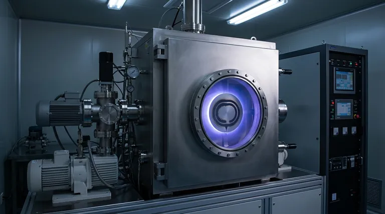
While the principle is straightforward, a high-performance magnetron sputtering system is a complex piece of equipment.
It requires a high-vacuum chamber, expensive vacuum pumps, precise gas flow controllers, and sophisticated power supplies. The initial capital investment and the expertise required to operate and maintain these systems can be significant.
Unwanted Substrate Heating
The sputtering process involves energetic particles bombarding the target, and both these particles and the sputtered atoms can transfer significant energy to the substrate.
This can cause unwanted heating, which may damage heat-sensitive substrates like plastics or certain electronic components. Managing this thermal load often requires dedicated substrate cooling systems.
Plasma Instability and Process Control
Maintaining a perfectly stable plasma is critical for achieving repeatable, uniform films.
Fluctuations in gas pressure, power, or the condition of the target surface can lead to instability. This demands precise control systems and regular maintenance to ensure consistent results, especially in high-volume industrial production.
Understanding the Trade-offs
It is crucial to view these problems not as deal-breakers, but as trade-offs for the technology's powerful benefits. Magnetron sputtering remains a dominant process for a reason.
Flexibility vs. Complexity
The ability to deposit a vast range of materials—from pure metals to complex alloys and ceramic compounds—is a primary advantage. This material independence is achieved at the cost of the system complexity required to control the process.
Film Quality vs. Process Constraints
Sputtered films are known for their exceptional density, purity, and adhesion to the substrate. The high energy of the sputtered atoms helps create a superior bond. This high quality is the payoff for managing challenges like target utilization and substrate heating.
Making the Right Decision for Your Application
Ultimately, the "problems" of magnetron sputtering only become true disadvantages if there is a mismatch between the technology and the goal.
- If your primary focus is depositing high-purity metals or complex alloys with excellent adhesion: Magnetron sputtering is an exceptional choice, and its challenges are well-understood and manageable engineering problems.
- If your primary focus is high-speed, low-cost coating of simple insulating materials: The slow deposition rate for dielectrics may be a significant barrier, and you should evaluate alternative methods like thermal evaporation.
- If your primary focus is working with a very limited budget or requires low-maintenance equipment: The high capital cost and operational complexity of sputtering systems could make it a less suitable option.
By understanding these specific challenges, you can properly engineer your process and determine if magnetron sputtering is the optimal tool to achieve your goals.
Summary Table:
| Problem | Description | Impact |
|---|---|---|
| Inefficient Target Use | Plasma erodes a 'racetrack' on the target. | Low material utilization (20-30%), higher consumable costs. |
| Target Poisoning | Reactive gases form a compound layer on the target. | Sudden drop in deposition rate, altered film composition. |
| Slow Dielectric Deposition | Charge buildup halts sputtering on insulating targets. | Requires complex RF systems, slower process. |
| High System Cost & Complexity | Requires vacuum chambers, pumps, and precise controls. | Significant initial investment and operational expertise. |
| Unwanted Substrate Heating | Energetic particles bombard the substrate. | Can damage heat-sensitive materials. |
Ready to Optimize Your Sputtering Process?
While magnetron sputtering has its challenges, they are manageable with the right expertise and equipment. KINTEK specializes in providing high-quality lab equipment and consumables for all your deposition needs. Our team can help you select the right system, manage process complexities, and maximize your material utilization.
Contact us today to discuss how we can support your laboratory's specific application and help you achieve superior film quality. Get in touch via our contact form to speak with an expert!
Visual Guide
Related Products
- Spark Plasma Sintering Furnace SPS Furnace
- RF PECVD System Radio Frequency Plasma-Enhanced Chemical Vapor Deposition RF PECVD
People Also Ask
- What is the process fundamentals of spark plasma sintering? Achieve Rapid, High-Density Material Consolidation
- What technical advantages does a Spark Plasma Sintering (SPS) furnace offer for LZP ceramics? Enhance Ionic Conductivity
- What is the pressure for spark plasma sintering? A Guide to Optimizing SPS Parameters
- What are the advantages of CAMI/SPS for W-Cu composite preparation? Reduce cycles from hours to seconds.
- Why are Spark Plasma Sintering (SPS) furnaces or hot presses utilized in the preparation of Li3PS4 solid electrolytes?

