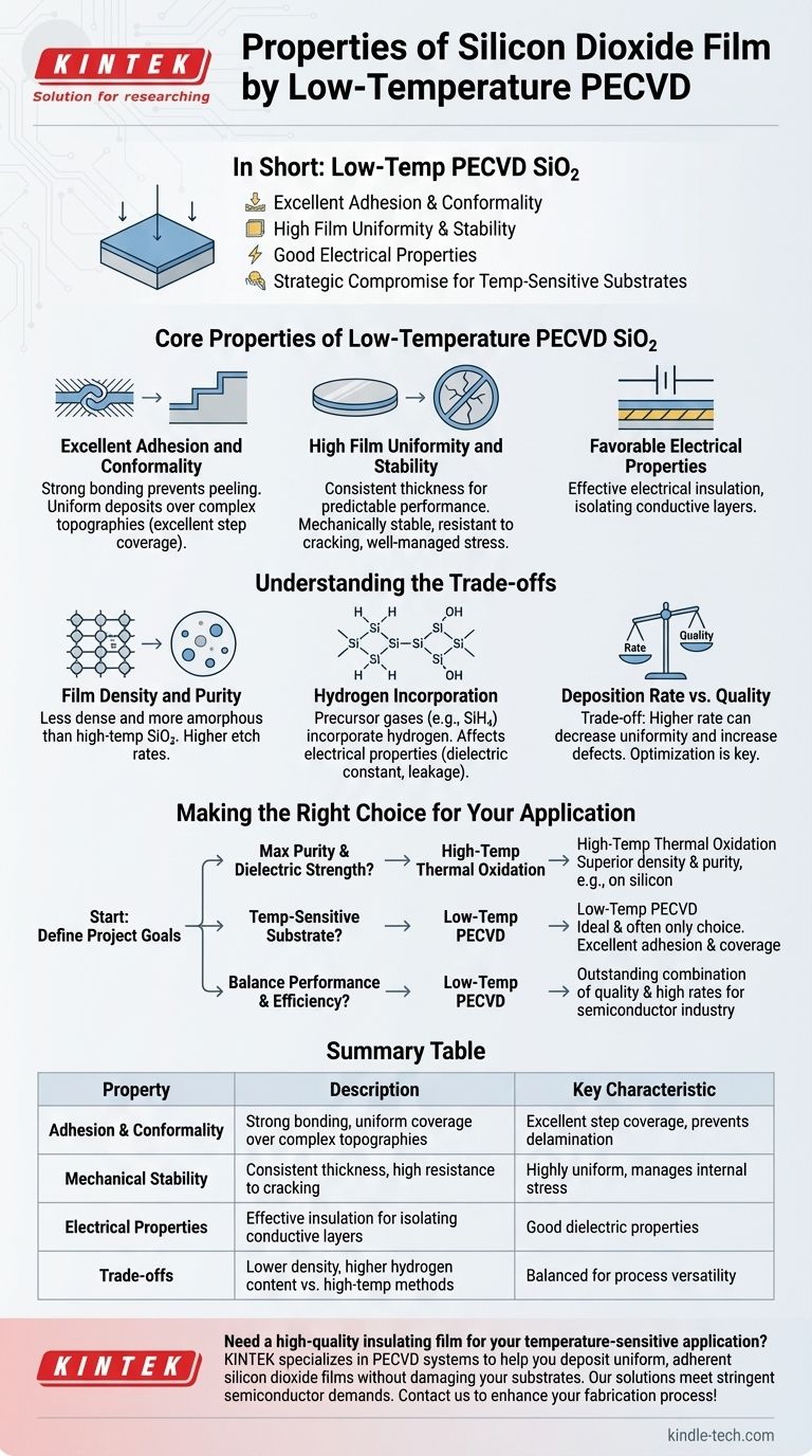
In short, silicon dioxide (SiO₂) films deposited by low-temperature Plasma-Enhanced Chemical Vapor Deposition (PECVD) are primarily characterized by their excellent adhesion to the substrate, high-quality uniform thickness, and good electrical properties. This process produces mechanically stable films that are resistant to cracking and can effectively cover complex surface topographies (step coverage).
The core takeaway is that low-temperature PECVD is a strategic compromise. It enables the deposition of a high-quality, functional SiO₂ film on temperature-sensitive materials where high-temperature methods would be destructive, trading absolute film purity for process versatility.
Core Properties of Low-Temperature PECVD SiO₂
Low-temperature PECVD is engineered to deliver a robust insulating layer without exposing the substrate to damaging heat. This results in a distinct set of valuable film characteristics.
Excellent Adhesion and Conformality
The plasma-enhanced nature of the process promotes strong chemical bonding between the film and the substrate surface. This results in excellent adhesion, preventing the film from peeling or delaminating.
Furthermore, these films exhibit excellent step coverage. This means the SiO₂ deposits uniformly over sharp edges and complex topographies on the substrate, which is critical for ensuring complete insulation in multi-layered devices.
High Film Uniformity and Stability
PECVD systems are capable of depositing films with highly uniform thickness across the entire substrate. This consistency is essential for predictable and reliable device performance.
The resulting films are also mechanically stable and show a high resistance to cracking. This indicates that the internal stress of the film is well-managed during the low-temperature deposition process.
Favorable Electrical Properties
For most applications, the primary function of SiO₂ is to serve as a dielectric or electrical insulator. Low-temperature PECVD films provide good electrical insulation, effectively isolating conductive layers from one another.
Understanding the Trade-offs of Low Temperature
While the properties are favorable, choosing a low-temperature process involves inherent trade-offs compared to high-temperature alternatives like thermal oxidation.
Film Density and Purity
Low-temperature PECVD films are typically less dense and have a more amorphous structure than SiO₂ grown at high temperatures. This lower density can result in a slightly higher etch rate in certain chemicals.
These films also tend to have a higher concentration of impurities, most notably hydrogen.
Hydrogen Incorporation
The precursor gases used in PECVD (like silane, SiH₄) contain hydrogen. At low deposition temperatures, not all hydrogen atoms are driven out of the film, becoming incorporated into the silicon dioxide matrix as Si-H or Si-OH bonds.
This incorporated hydrogen can affect the film's electrical properties, such as dielectric constant and leakage current. For many applications this is acceptable, but for high-performance gate dielectrics, it can be a limiting factor.
Deposition Rate vs. Quality
There is a fundamental trade-off between the deposition rate and the final film quality. Increasing the rate for higher throughput can sometimes lead to decreased uniformity and higher defect density.
Optimizing the process for industrial applications involves finding the ideal balance that meets both throughput demands and performance specifications.
Making the Right Choice for Your Application
Selecting the right deposition method depends entirely on the constraints and goals of your specific project.
- If your primary focus is maximum film purity and dielectric strength: A high-temperature process like thermal oxidation (if depositing on silicon) is superior, as it produces a denser, purer SiO₂.
- If your primary focus is depositing an insulating layer on a temperature-sensitive substrate: Low-temperature PECVD is the ideal and often only choice, providing excellent adhesion and coverage without damaging underlying materials or devices.
- If your primary focus is balancing performance with manufacturing efficiency: Low-temperature PECVD offers an outstanding combination of good film quality and high deposition rates, making it a workhorse of the semiconductor industry.
By understanding these characteristics, you can effectively leverage low-temperature PECVD to solve complex fabrication challenges.
Summary Table:
| Property | Description | Key Characteristic |
|---|---|---|
| Adhesion & Conformality | Strong bonding to substrate, uniform coverage over complex topographies | Excellent step coverage, prevents delamination |
| Mechanical Stability | Consistent film thickness, high resistance to cracking | Highly uniform, manages internal stress |
| Electrical Properties | Effective electrical insulation for isolating conductive layers | Good dielectric properties |
| Trade-offs | Lower density, higher hydrogen content vs. high-temperature methods | Balanced for process versatility |
Need a high-quality insulating film for your temperature-sensitive application? KINTEK specializes in lab equipment and consumables, including PECVD systems, to help you deposit uniform, adherent silicon dioxide films without damaging your substrates. Our solutions are designed to meet the stringent demands of semiconductor and advanced materials research. Contact us today to discuss how we can enhance your fabrication process and achieve reliable performance!
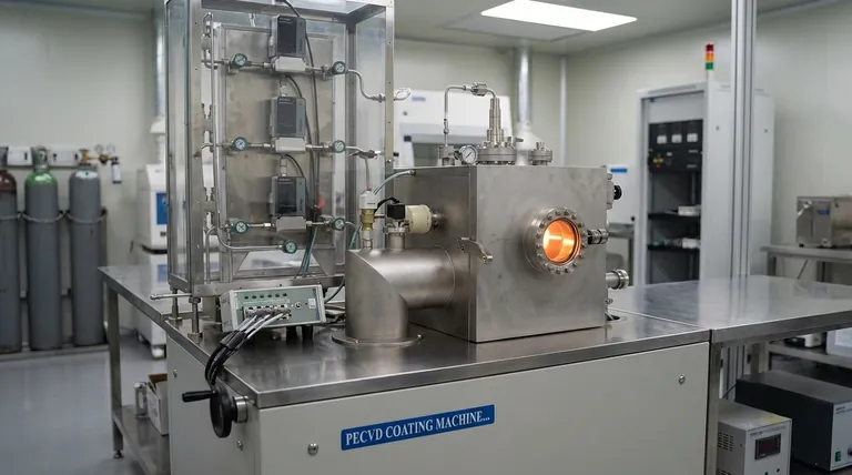
Visual Guide
Related Products
- Chemical Vapor Deposition CVD Equipment System Chamber Slide PECVD Tube Furnace with Liquid Gasifier PECVD Machine
- Inclined Rotary Plasma Enhanced Chemical Vapor Deposition PECVD Equipment Tube Furnace Machine
- RF PECVD System Radio Frequency Plasma-Enhanced Chemical Vapor Deposition RF PECVD
- Inclined Rotary Plasma Enhanced Chemical Vapor Deposition PECVD Equipment Tube Furnace Machine
- Custom CVD Diamond Coating for Lab Applications
People Also Ask
- What types of substrates are used in CVD to facilitate graphene films? Optimize Graphene Growth with the Right Catalyst
- What is the chemical vapor deposition growth process? Build Superior Thin Films from the Atom Up
- What are the core advantages of PE-CVD in OLED encapsulation? Protect Sensitive Layers with Low-Temp Film Deposition
- What happens during deposition chemistry? Building Thin Films from Gaseous Precursors
- Why is Chemical Vapor Deposition (CVD) equipment uniquely suited for constructing hierarchical superhydrophobic structures?


