In short, thermal evaporation is a foundational technology for creating thin films, most commonly used to deposit metal layers for electronics, create reflective optical coatings, and apply decorative finishes. Its applications range from the conductive layers in OLED displays and solar cells to the reflective surfaces on automotive headlights and the metallic sheen on cosmetic packaging.
Thermal evaporation is a straightforward, cost-effective vacuum deposition process. Its value lies in its ability to quickly deposit high-purity films of materials with relatively low melting points, making it an indispensable tool for specific applications in electronics and optics where simplicity and material purity are paramount.
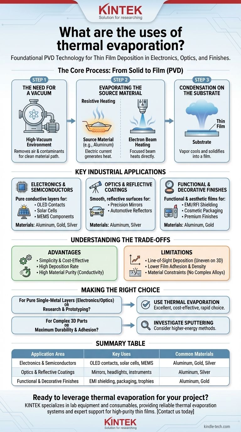
The Core Process: From Solid to Film
Thermal evaporation is a type of Physical Vapor Deposition (PVD). The principle is elegantly simple and mirrors the natural water cycle, but it occurs within a controlled, high-vacuum environment.
The Need for a Vacuum
The entire process takes place in a high-vacuum chamber. This vacuum is critical because it removes air and other gas molecules that could collide with the evaporated material, ensuring a clean and direct path from the source to the target.
Evaporating the Source Material
A source material, such as a pellet of aluminum or gold, is placed in a container called a crucible. This crucible is heated until the source material turns from a solid directly into a vapor. This heating is typically achieved through one of two methods:
- Resistive Heating: An electric current is passed through a refractory metal boat or filament holding the material, generating heat.
- Electron Beam Heating: A focused beam of high-energy electrons heats the source material directly.
Condensation on the Substrate
This vapor cloud expands throughout the chamber and lands on a cooler surface, known as the substrate. Upon contact, the vapor rapidly cools and condenses back into a solid, forming a thin, uniform film across the substrate's surface.
Key Industrial Applications
The simplicity and effectiveness of this process have made it a staple in numerous high-tech and consumer industries.
Electronics and Semiconductors
This is the most common application area. The ability to deposit pure, conductive metal layers is essential for modern electronics.
- Electrical Contacts: Creating contacts and interconnects on OLEDs, thin-film transistors, and other semiconductor devices using metals like aluminum or silver.
- Solar Cells: Depositing metal bonding layers that are critical for extracting electrical current.
- Microelectromechanical Systems (MEMS): Building up the microscopic components used in sensors and actuators.
Optics and Reflective Coatings
Thermal evaporation excels at creating highly reflective surfaces. The process produces a smooth film that is ideal for managing light.
- Reflectors: Manufacturing light reflectors for automotive headlights, medical lighting, and aerospace equipment.
- Mirrors: Creating the reflective layers on precision mirrors for telescopes and other optical instruments.
Functional and Decorative Finishes
The process is also widely used to apply films that serve a functional or purely aesthetic purpose.
- EMI/RFI Shielding: Depositing a thin layer of metal onto plastic housings for electronic devices to block electromagnetic or radio-frequency interference.
- Decorative Coatings: Applying a metallic finish to items like cosmetic closures, trophies, and sporting goods to give them a premium look at a low cost.
Understanding the Trade-offs
No single technology is perfect for every job. Choosing thermal evaporation requires understanding its distinct advantages and limitations.
The Advantage: Simplicity and Cost
Thermal evaporation systems are mechanically simpler and generally less expensive than other PVD methods like sputtering. This makes the technology highly accessible for research, prototyping, and cost-sensitive production.
The Advantage: High Deposition Rate and Purity
For many materials, especially metals with low melting points like aluminum, the process is very fast. Because the material is simply evaporated, the resulting film maintains a very high level of purity, which is critical for electrical conductivity.
The Limitation: Line-of-Sight Deposition
The evaporated material travels in a straight line from the source to the substrate. This line-of-sight nature means it is difficult to evenly coat complex, three-dimensional shapes without sophisticated rotating fixtures.
The Limitation: Film Adhesion and Density
Because the evaporated atoms arrive at the substrate with relatively low energy, the resulting films can be less dense and have weaker adhesion compared to films from more energetic processes like sputtering. While the adhesion is good enough for many applications, it may not be suitable for high-wear or high-stress environments.
The Limitation: Material Constraints
The process is best suited for materials that can be heated to a vapor state without decomposing or reacting chemically. Complex alloys or compounds can be difficult to deposit with consistent stoichiometry.
Making the Right Choice for Your Application
To determine if thermal evaporation is the correct approach, consider your primary goal.
- If your primary focus is depositing pure, single-metal layers for electronics or optics: Thermal evaporation is an excellent, cost-effective, and rapid choice.
- If your primary focus is on research, development, or rapid prototyping of thin films: The simplicity and low cost of this technology make it an ideal starting point.
- If your primary focus is coating complex 3D parts or achieving maximum durability and adhesion: You should investigate higher-energy deposition methods like magnetron sputtering.
Ultimately, understanding the fundamental principles of thermal evaporation allows you to leverage its strengths for the precise applications where it truly excels.
Summary Table:
| Application Area | Key Uses | Common Materials |
|---|---|---|
| Electronics & Semiconductors | OLED contacts, solar cell layers, MEMS components | Aluminum, Gold, Silver |
| Optics & Reflective Coatings | Mirrors, automotive headlights, precision instruments | Aluminum, Silver |
| Functional & Decorative Finishes | EMI shielding, cosmetic packaging, trophies | Aluminum, Gold |
Ready to leverage thermal evaporation for your project? KINTEK specializes in lab equipment and consumables, providing reliable thermal evaporation systems and expert support to help you achieve high-purity thin films for electronics, optics, and more. Contact us today to discuss your specific laboratory needs and discover the right solution for your application!
Visual Guide
Related Products
- Molybdenum Tungsten Tantalum Evaporation Boat for High Temperature Applications
- Aluminized Ceramic Evaporation Boat for Thin Film Deposition
- Evaporation Boat for Organic Matter
- Electron Beam Evaporation Coating Tungsten Crucible and Molybdenum Crucible for High Temperature Applications
- High Purity Pure Graphite Crucible for Evaporation
People Also Ask
- What are thermal evaporation sources? Key Types and How to Choose the Right One
- What is thermal evaporation used to deposit? A Guide to Metals, Compounds, and Key Applications
- What is the widely used boat made of in thermal evaporation? Choosing the Right Material for High-Purity Deposition
- What is the thermal evaporation method in thin film? A Guide to Simple, Cost-Effective PVD
- What is the difference between thermal evaporation and e beam evaporation? Choose the Right Method for Your Thin Film