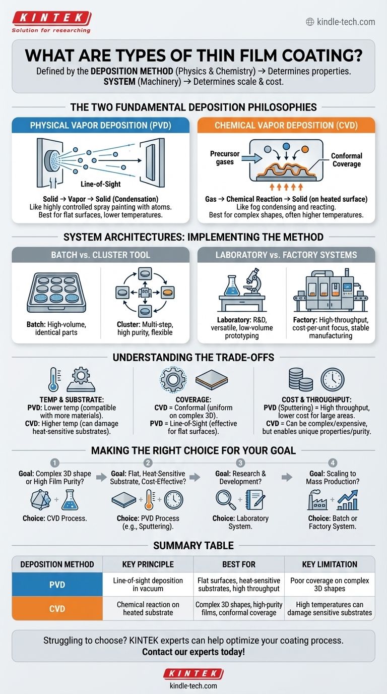
At its core, a "type" of thin film coating is defined by how it is created. While the machinery can be categorized by size and throughput, the fundamental distinction lies in the deposition method, which primarily falls into two categories: Physical Vapor Deposition (PVD) and Chemical Vapor Deposition (CVD). These methods determine the film's properties, performance, and suitability for your specific application.
The most critical takeaway is to distinguish between the deposition method (the physics and chemistry of film creation) and the deposition system (the machinery that performs the method). Your choice of method dictates the film's characteristics, while the system dictates the scale and cost of production.
The Two Fundamental Deposition Philosophies
The world of thin film coatings is built on two primary approaches for depositing material onto a substrate. Understanding this distinction is the first step in making an informed decision.
Physical Vapor Deposition (PVD)
Physical Vapor Deposition (PVD) is a process where a solid material is physically converted into a vapor, transported through a vacuum, and condensed onto a substrate as a thin film. Think of it like a highly controlled form of spray painting, but with atoms instead of paint droplets.
The material is "liberated" from a solid source, most commonly through methods like sputtering (bombarding the source with ions) or thermal evaporation (heating the source until it vaporizes).
Because the vapor travels in a straight line from the source to the substrate, PVD is considered a line-of-sight process. It works best for coating flat or gently curved surfaces.
Chemical Vapor Deposition (CVD)
Chemical Vapor Deposition (CVD) operates through a fundamentally different principle. In this method, precursor gases are introduced into a chamber, where they react and decompose on the surface of a heated substrate, forming the desired solid film.
Imagine a hot surface causing a surrounding fog to condense and form a uniform layer of ice; CVD is a highly engineered version of this concept.
Because the precursor gases can flow around and into complex geometries, CVD provides excellent conformal coverage. This means it can uniformly coat intricate, three-dimensional structures, which is a significant advantage over PVD.
How Deposition Methods Are Implemented: System Architectures
The deposition method (PVD or CVD) is executed by a piece of equipment. The architecture of this system is chosen based on throughput, research needs, and manufacturing scale.
Batch vs. Cluster Tool Systems
Batch systems are designed to process multiple substrates, or wafers, simultaneously in a single chamber. This is efficient for high-volume production of identical parts.
Cluster tools, by contrast, are multi-chamber systems where a single substrate is moved by a central robot between different process chambers. This allows for complex, multi-step coating processes without breaking the vacuum, ensuring high film purity.
Laboratory vs. Factory Systems
Laboratory or bench-top systems are small, flexible tools designed for research and development (R&D) or low-volume prototyping. Their priority is versatility and experimentation.
Factory or freestanding systems are large-scale industrial machines optimized for high-throughput, repeatable manufacturing. These systems prioritize cost per unit, uptime, and process stability over flexibility.
Understanding the Trade-offs
Choosing a coating type is not about finding the "best" one, but the right one for your goal. This involves balancing performance, material compatibility, and cost.
Temperature and Substrate Compatibility
Many CVD processes require very high temperatures to drive the chemical reactions, which can damage heat-sensitive substrates like plastics or certain semiconductor devices.
PVD processes generally operate at much lower temperatures, making them compatible with a wider range of materials.
Conformal Coverage vs. Line-of-Sight
If you need to uniformly coat a complex part with deep trenches or intricate features, the conformal nature of CVD is often a necessity.
For flat surfaces like architectural glass, solar cells, or display screens, the line-of-sight deposition of PVD is highly effective and economical.
Cost, Throughput, and Complexity
Generally, PVD systems (especially sputtering) are known for their robustness, high throughput, and lower cost for large-area coatings, making them a workhorse of many industries.
CVD can be more complex and expensive due to the need to handle precursor gases and often higher temperatures, but it enables the creation of films with properties and purity that PVD cannot achieve.
Making the Right Choice for Your Goal
Your application's requirements should be the ultimate guide for selecting a thin film coating method and system.
- If your primary focus is coating a complex 3D shape or achieving high film purity: A CVD process is likely the superior choice for its conformal coverage and chemical precision.
- If your primary focus is coating a flat, heat-sensitive substrate cost-effectively: A PVD process, likely sputtering, will provide an excellent balance of performance and cost.
- If your primary focus is research and development: A flexible laboratory system will allow you to experiment with different materials and processes.
- If your primary focus is scaling to mass production: A dedicated batch or factory system will be required to meet throughput and cost targets.
Ultimately, understanding the physics of the deposition method is the key to predicting the final properties of your thin film coating.
Summary Table:
| Deposition Method | Key Principle | Best For | Key Limitation |
|---|---|---|---|
| PVD (Physical Vapor Deposition) | Line-of-sight deposition in a vacuum | Flat surfaces, heat-sensitive substrates, high throughput | Poor coverage on complex 3D shapes |
| CVD (Chemical Vapor Deposition) | Chemical reaction on a heated substrate | Complex 3D shapes, high-purity films, conformal coverage | High temperatures can damage sensitive substrates |
Struggling to choose the right thin film coating for your application? The experts at KINTEK are here to help. We specialize in lab equipment and consumables for all your thin film deposition needs, from research-grade PVD and CVD systems to high-throughput production solutions. Our team can guide you to the optimal method and equipment for your specific substrate, desired film properties, and production scale. Let's optimize your coating process together — contact our experts today!
Visual Guide
Related Products
- Aluminized Ceramic Evaporation Boat for Thin Film Deposition
- Electron Beam Evaporation Coating Oxygen-Free Copper Crucible and Evaporation Boat
- Tungsten Evaporation Boat for Thin Film Deposition
- Molybdenum Tungsten Tantalum Evaporation Boat for High Temperature Applications
- Aluminum-Plastic Flexible Packaging Film for Lithium Battery Packaging
People Also Ask
- What is thin film deposition? Unlock Advanced Surface Engineering for Your Materials
- Why is an alumina boat selected for catalyst precursors? Ensure Sample Purity at 1000 °C
- What are the applications of thin films deposition? Unlock New Possibilities for Your Materials
- What is the source of evaporation for thin film? Choosing Between Thermal and E-Beam Methods
- What is the chemical method for thin film deposition? Build Films from the Molecular Level Up


