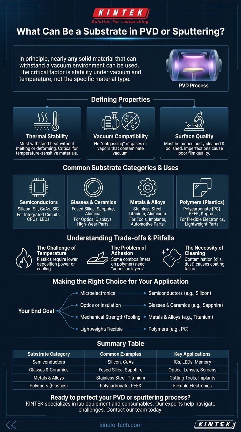
In principle, nearly any solid material that can withstand a vacuum environment can be used as a substrate in Physical Vapor Deposition (PVD) and sputtering. The selection is most often dictated by the final application of the coated part, with common examples including semiconductor wafers for electronics, glass for optics, and metals for tools.
The critical factor in choosing a substrate is not its specific material type, but its ability to remain stable under the vacuum and temperature conditions of the PVD process. Your choice is ultimately guided by the demands of your final product and the physical limits of the deposition environment.
The Defining Properties of a Suitable Substrate
A material's suitability as a substrate hinges on a few core physical and chemical properties. Ignoring these can lead to failed depositions, poor film quality, and contaminated equipment.
Thermal Stability
The PVD process, especially sputtering, generates significant heat. The substrate must be able to withstand these temperatures without melting, deforming, or breaking down.
For example, high-power sputtering onto a low-melting-point plastic would be disastrous. This is why process parameters are often adjusted for temperature-sensitive materials.
Vacuum Compatibility
PVD occurs in a high-vacuum chamber. The substrate cannot release gases or vapors—a phenomenon known as outgassing—as this will contaminate the vacuum and interfere with the film deposition.
Porous materials like wood, unsealed ceramics, or many soft plastics are generally unsuitable because they trap air and moisture, which they release under vacuum.
Surface Quality
The deposited thin film will replicate the surface it is grown on. A rough, dirty, or defective substrate surface will almost certainly result in a rough, poorly-adhering, and defective film.
Therefore, substrates must be meticulously cleaned and are often polished to a very smooth finish before being placed in the deposition chamber.
Common Substrate Categories and Their Uses
While the possibilities are broad, most substrates fall into one of a few key categories, each tied to specific industries and applications.
Semiconductors
These materials are the foundation of the entire microelectronics industry. The substrate is not just a carrier but an active part of the final device.
- Examples: Silicon (Si), Gallium Arsenide (GaAs), Silicon Carbide (SiC)
- Applications: Integrated circuits, CPUs, memory chips, LEDs.
Glasses and Ceramics
Chosen for their optical transparency, electrical insulation, or extreme hardness and temperature resistance.
- Examples: Fused Silica, Borosilicate Glass, Sapphire, Alumina (Al₂O₃)
- Applications: Optical lenses and filters, display screens, electronic circuit boards, high-wear components.
Metals and Alloys
Used when the final product requires mechanical strength, durability, or conductivity. The coatings applied often enhance wear resistance, reduce friction, or provide a decorative finish.
- Examples: Stainless Steel, Titanium, Aluminum, Copper
- Applications: Cutting tools, medical implants, automotive parts, decorative hardware.
Polymers (Plastics)
Coating plastics is possible but requires special care. The low melting points and tendency to outgas mean that low-temperature deposition processes must be used.
- Examples: Polycarbonate (PC), Kapton, PEEK
- Applications: Flexible electronics, lightweight optical components, metallized packaging films.
Understanding the Trade-offs and Pitfalls
Selecting a substrate is not without its challenges. Understanding the limitations is key to a successful coating process.
The Challenge of Temperature
If you must coat a temperature-sensitive material like a common plastic, you are constrained. You will need to use lower deposition power, which slows down the process, and potentially add substrate cooling, which complicates the chamber setup.
The Problem of Adhesion
A film is only as good as its bond to the substrate. Some material combinations have naturally poor adhesion. For instance, depositing a metal onto a polymer can be difficult without first using a special "adhesion layer" to act as a glue between the substrate and the final film.
The Necessity of Cleaning
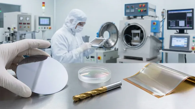
Any contamination on the substrate surface—such as oils, dust, or oxides—will be a point of failure for the coating. Substrate cleaning is a multi-step, critical process that cannot be overlooked. For materials like silicon wafers, this cleaning is performed in a cleanroom environment.
Making the Right Choice for Your Application
Your choice of substrate is determined entirely by your end goal. The substrate is the foundation upon which your thin film's performance is built.
- If your primary focus is microelectronics: Your choice is almost always a semiconductor wafer, typically silicon.
- If your primary focus is optics or insulation: You will use high-quality glass, quartz, or a technical ceramic like sapphire.
- If your primary focus is mechanical strength or tooling: Your substrate will be a hard metal or alloy, such as steel or titanium.
- If your primary focus is lightweight or flexible parts: You can use polymers, but you must design your PVD process carefully around their temperature and vacuum limitations.
Ultimately, the right substrate is one that meets your application's needs while being compatible with the physics of the deposition process.
Summary Table:
| Substrate Category | Common Examples | Key Applications |
|---|---|---|
| Semiconductors | Silicon (Si), Gallium Arsenide (GaAs) | Integrated Circuits, LEDs, Memory Chips |
| Glasses & Ceramics | Fused Silica, Sapphire, Alumina | Optical Lenses, Display Screens, Circuit Boards |
| Metals & Alloys | Stainless Steel, Titanium, Aluminum | Cutting Tools, Medical Implants, Automotive Parts |
| Polymers (Plastics) | Polycarbonate (PC), Kapton, PEEK | Flexible Electronics, Lightweight Optics |
Ready to perfect your PVD or sputtering process? Selecting the right substrate is critical for achieving high-quality, durable thin films. At KINTEK, we specialize in providing the precise lab equipment and consumables you need for successful deposition. Our experts can help you navigate the challenges of thermal stability, adhesion, and surface preparation. Let's build the foundation for your next breakthrough—contact our team today to discuss your specific application requirements.
Visual Guide
Related Products
- Vacuum Hot Press Furnace Machine for Lamination and Heating
- Split Chamber CVD Tube Furnace with Vacuum Station Chemical Vapor Deposition System Equipment Machine
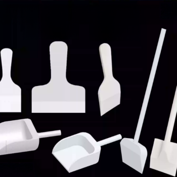
- Custom PTFE Teflon Parts Manufacturer for Acid and Alkali Resistant Chemical Powder Material Scoops
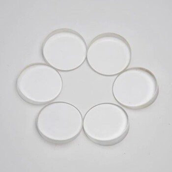
- Optical Window Glass Substrate Wafer CaF2 Substrate Window Lens
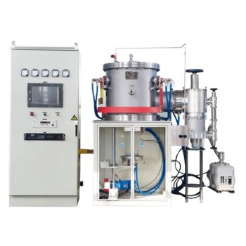
- Graphite Vacuum Continuous Graphitization Furnace
People Also Ask
- What are the advantages and disadvantages of hot stamping? Unlock Ultra-High Strength for Automotive Parts
- What is the purpose of laminating? Protect and Enhance Your Documents for Long-Term Use
- What is hot press forging? Creating Complex, High-Strength Metal Components
- What is hot press moulding? Achieve Superior Density and Complex Shapes with Heat and Pressure
- What is the advantage by using hot press forming? Achieve Stronger, More Complex Parts