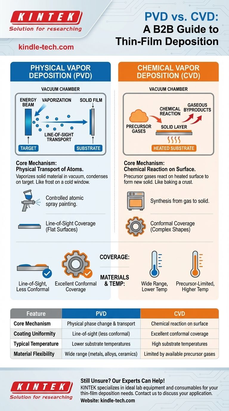
At their core, Physical Vapor Deposition (PVD) and Chemical Vapor Deposition (CVD) are two distinct methods for applying high-performance thin films to a surface. PVD is a physical process where a solid material is vaporized in a vacuum and condenses onto a target, much like water vapor forms frost on a cold window. In contrast, CVD is a chemical process where precursor gases are introduced into a chamber and react on a heated surface to form an entirely new solid layer, leaving gaseous byproducts behind.
The fundamental difference lies in how the coating material arrives and forms on the surface. PVD physically transports atoms from a source to the substrate, while CVD uses chemical reactions from precursor gases to grow a new layer directly on the substrate itself.
The Core Mechanism: Physical vs. Chemical
To truly understand which process to use, you must grasp their foundational differences in operation. The name of each process is the most important clue.
How PVD Works: A Line-of-Sight Transfer
Physical Vapor Deposition is fundamentally a phase-change process. It moves material from a solid source to a solid film on your part.
The process involves placing a solid source material (the "target") and the component to be coated (the "substrate") into a vacuum chamber. A high-energy source, such as an electron beam or ion bombardment, vaporizes atoms from the target. These vaporized atoms travel in a straight line through the vacuum and condense on the substrate, forming a thin, solid film.
Think of it as a highly controlled form of spray painting at the atomic level. The "paint" (vaporized atoms) only coats the surfaces it can see from the source.
How CVD Works: Building a Layer from Gas
Chemical Vapor Deposition is a process of synthesis. It doesn't just move material; it creates a new solid material on the substrate's surface through a chemical reaction.
In this method, one or more volatile precursor gases are introduced into a vacuum chamber containing the heated substrate. The heat provides the energy needed to trigger a chemical reaction or decomposition of the gases directly on the hot surface. This reaction forms the desired solid coating and produces gaseous byproducts, which are then pumped out of the chamber.
This is more analogous to baking a crust onto a piece of bread. The ingredients (gases) surround the entire part, and the crust (coating) forms everywhere the surface is hot enough.
Understanding the Trade-offs
The choice between PVD and CVD is not about which is "better" but which is better suited for a specific outcome. The core mechanism of each process creates distinct advantages and disadvantages.
Conformal Coverage: The CVD Advantage
Because the precursor gases in CVD can flow and surround a component, the resulting coating is highly conformal. This means it can uniformly coat complex, three-dimensional shapes, including internal surfaces and intricate geometries.
Line-of-Sight Deposition: The PVD Reality
PVD is a line-of-sight process. The vaporized material travels in a straight path, meaning it struggles to coat undercuts, sharp corners, or internal channels without complex part rotation. This makes it ideal for coating flatter surfaces.
Material and Temperature Constraints
CVD processes are limited to materials for which suitable, stable, and volatile precursor gases exist. It also typically requires very high substrate temperatures to drive the chemical reactions, which can damage sensitive materials.
PVD, on the other hand, can deposit a vast range of materials, including pure metals, alloys, and ceramics, that do not have gaseous precursors. While the source is very hot, the substrate can often be kept at a lower temperature than in traditional CVD processes.
Making the Right Choice for Your Application
Selecting the correct deposition technique requires aligning the process capabilities with your primary engineering goal.
- If your primary focus is coating a complex, 3D shape uniformly: CVD is the superior choice due to its excellent conformal coverage.
- If your primary focus is depositing a pure metal, alloy, or hard ceramic onto a relatively flat surface: PVD offers excellent control and material flexibility.
- If your primary focus is coating a temperature-sensitive material: A low-temperature PVD process or a specialized variant like Plasma-Enhanced CVD (PECVD) should be investigated.
Understanding the fundamental difference between these two powerful techniques—physical transport versus chemical reaction—is the first step toward selecting the optimal process for your specific engineering goal.
Summary Table:
| Feature | Physical Vapor Deposition (PVD) | Chemical Vapor Deposition (CVD) |
|---|---|---|
| Core Mechanism | Physical phase change and transport | Chemical reaction on surface |
| Coating Uniformity | Line-of-sight (less conformal) | Excellent conformal coverage |
| Typical Temperature | Lower substrate temperatures | High substrate temperatures |
| Material Flexibility | Wide range (metals, alloys, ceramics) | Limited by available precursor gases |
Still unsure whether PVD or CVD is right for your project? Our experts at KINTEK can help you navigate these complex decisions. We specialize in providing the ideal lab equipment and consumables for your specific thin-film deposition needs. Contact our team today to discuss your application and discover how our solutions can enhance your laboratory's capabilities and efficiency.
Visual Guide