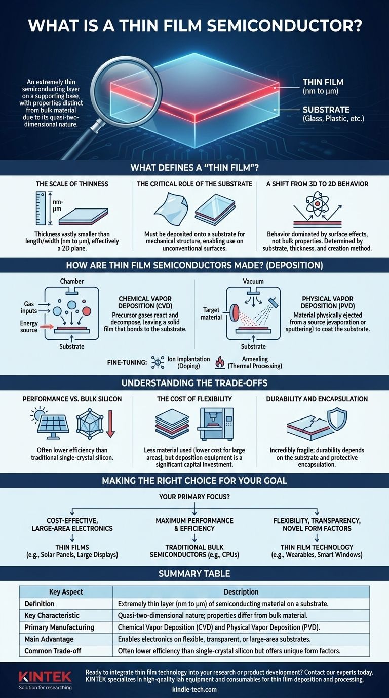
At its core, a thin film semiconductor is an extremely thin layer of a semiconducting material deposited onto a supporting base, or substrate. This layer's thickness ranges from a few nanometers to several micrometers, a scale so small that its physical and electronic properties differ significantly from the same material in its bulk form. This unique, quasi-two-dimensional nature is what makes the technology distinct and powerful.
While traditional semiconductors are rigid, bulky, and fabricated from solid crystals, thin film semiconductors apply these electronic properties to unconventional surfaces. This unlocks applications like flexible displays, large-area solar panels, and transparent electronics that are physically impossible with conventional methods.
What Defines a "Thin Film"?
The term "thin film" is not just about being small; it describes a fundamental shift in how the material behaves. This behavior is dictated by its unique geometry and its relationship with the surface it sits on.
The Scale of Thinness
A thin film is a layer of material whose thickness is vastly smaller than its length and width. This dimension is measured in nanometers (billionths of a meter) or micrometers (millionths of a meter), making it effectively a two-dimensional plane.
The Critical Role of the Substrate
Unlike a self-supporting silicon wafer, a thin film cannot exist on its own. It must be deposited onto a substrate, which provides mechanical structure. This substrate can be anything from glass and plastic to metal, allowing semiconducting properties to be added to a huge variety of materials.
A Shift from 3D to 2D Behavior
Because one dimension (thickness) is suppressed, the material's behavior is dominated by surface effects rather than its bulk properties. The properties of the final film are a direct result of the substrate material, the film's thickness, and the method used to create it.
How Are Thin Film Semiconductors Made?
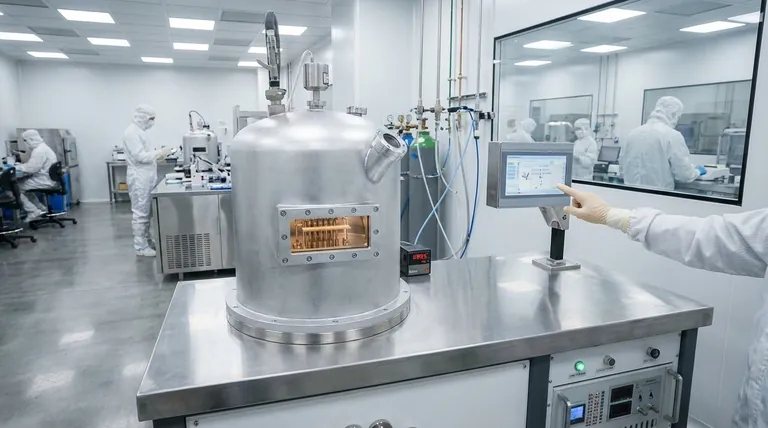
Thin film semiconductors are not carved from a larger block; they are built up atom by atom in highly controlled environments. This process is known as deposition.
Chemical Vapor Deposition (CVD)
In CVD, precursor gases are introduced into a reaction chamber. An energy source causes these gases to react and decompose, leaving behind a solid film that bonds to the substrate's surface. It's analogous to how steam condenses into a layer of frost on a cold window.
Physical Vapor Deposition (PVD)
PVD is a more mechanical process. Material is physically ejected from a source or "target" and travels through a vacuum to coat the substrate. This is often done through evaporation (boiling the material) or sputtering (bombarding the target with ions to knock atoms loose).
Fine-Tuning the Film
After the initial deposition, other processes are used to refine the film's properties. Ion implantation can be used to precisely introduce impurities (doping), while annealing (thermal processing in a vacuum) helps improve the crystalline structure and electrical characteristics of the film.
Understanding the Trade-offs
The unique advantages of thin films come with important trade-offs. Objectively understanding these limitations is key to using the technology effectively.
Performance vs. Bulk Silicon
Thin film semiconductors, particularly in applications like solar cells, often exhibit lower efficiency than their traditional, single-crystal silicon counterparts. The less-ordered atomic structure of many deposited films can impede electron flow compared to a perfect crystal lattice.
The Cost of Flexibility
While using less material makes thin films cheaper for large areas, the deposition equipment itself (like CVD or PVD reactors) represents a significant capital investment. The choice of deposition method directly impacts the final product's cost, quality, and uniformity.
Durability and Encapsulation
The film itself is incredibly fragile due to its thinness. Its durability is almost entirely dependent on the substrate it is on and the protective layers (encapsulation) applied over it. Without proper protection, thin films are highly susceptible to scratches, chemical damage, and environmental degradation.
Making the Right Choice for Your Goal
The decision between a thin film and a traditional bulk semiconductor is not about which is "better," but which is right for the job.
- If your primary focus is cost-effective, large-area electronics: Thin films are the superior choice for applications like solar panels or large displays where minimizing material usage per square meter is critical.
- If your primary focus is maximum performance and efficiency: Traditional bulk semiconductors, such as single-crystal silicon wafers, remain the standard for high-density, high-speed components like CPUs.
- If your primary focus is flexibility, transparency, or novel form factors: Thin film technology is the only viable path, enabling integration onto plastics, glass, and other materials for wearable sensors, smart windows, or flexible screens.
By understanding its function as a surface-based technology, you can effectively leverage the unique capabilities of thin film semiconductors for the right application.
Summary Table:
| Key Aspect | Description |
|---|---|
| Definition | An extremely thin layer (nanometers to micrometers) of semiconducting material deposited on a substrate. |
| Key Characteristic | Quasi-two-dimensional nature; properties differ significantly from bulk material. |
| Primary Manufacturing | Chemical Vapor Deposition (CVD) and Physical Vapor Deposition (PVD). |
| Main Advantage | Enables electronics on flexible, transparent, or large-area substrates. |
| Common Trade-off | Often lower efficiency than single-crystal silicon but offers unique form factors. |
Ready to integrate thin film technology into your research or product development?
KINTEK specializes in providing the high-quality lab equipment and consumables essential for thin film deposition and processing. Whether you are developing flexible electronics, advanced solar cells, or novel sensors, our expertise and reliable products support your innovation from R&D to production.
Contact our experts today to discuss how we can help you achieve your project goals with the right tools and materials.
Visual Guide
Related Products
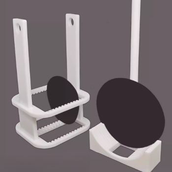
- Customizable PTFE Wafer Carriers for Semiconductor and Lab Applications
- Custom PTFE Wafer Holders for Lab and Semiconductor Processing
- Thin-Layer Spectral Electrolysis Electrochemical Cell
- Aluminum-Plastic Flexible Packaging Film for Lithium Battery Packaging
People Also Ask
- What is the function of a customized PTFE cap in IL-TEM? Bridge the Gap Between Microscopy and Electrochemistry
- Is PTFE corrosion resistant? Discover the Ultimate Chemical Resistance for Your Lab
- Why is PTFE wire used for hanging metal specimens in biodiesel corrosion tests? Ensure Pure Experimental Results
- Why are PTFE wafer fixtures used after diamond nucleation? Ensure Purity and Protect Fragile Nucleation Layers
- Why is slender PTFE tubing necessary for flow control in multi-channel catalyst aging? Ensure Equal Gas Distribution