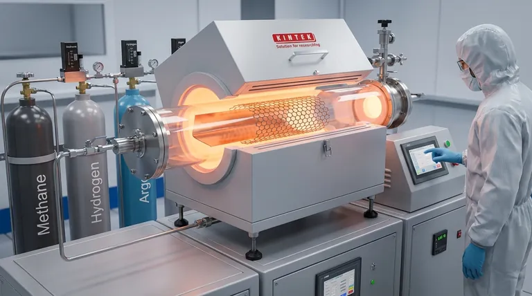
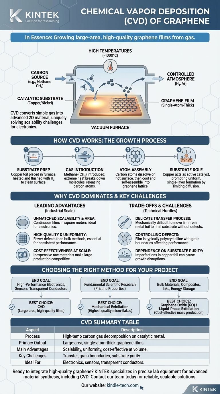
In essence, chemical deposition of graphene is a process for growing high-quality, large-area films of graphene from a gas. Known as Chemical Vapor Deposition (CVD), this technique involves heating a metal substrate, typically copper or nickel, in a vacuum furnace and introducing a carbon-containing gas like methane. At high temperatures, the gas decomposes, and carbon atoms assemble on the metal surface, forming a continuous, single-atom-thick layer of graphene.
Chemical Vapor Deposition (CVD) is the dominant industrial method for producing graphene because it uniquely solves the challenge of scalability. It allows for the creation of large, high-quality sheets suitable for electronics, a feat not possible with other common methods.
How Chemical Vapor Deposition (CVD) Works
To understand why CVD is so pivotal, we must first look at the mechanics of the process. It is a highly controlled, multi-step procedure that transforms simple gas into an advanced two-dimensional material.
The Core Components
The process occurs inside a specialized furnace chamber and requires four key ingredients:
- A catalytic substrate, most commonly a thin foil of copper.
- A carbon source, which is a hydrocarbon gas like methane (CH₄).
- High temperatures, typically around 1000°C (1832°F).
- A controlled atmosphere of other gases, like hydrogen and argon.
The Step-by-Step Growth Process
The synthesis of a graphene film follows a precise sequence. First, the copper foil is placed inside the furnace, which is then heated to the target temperature while being flushed with hydrogen gas to clean and prepare the metal's surface.
Next, a small, controlled amount of methane is introduced into the chamber. The extreme heat breaks the methane molecules apart, releasing individual carbon atoms.
These carbon atoms dissolve onto the hot surface of the copper foil. As the system is carefully cooled, the carbon atoms precipitate and self-assemble into graphene's signature hexagonal honeycomb lattice directly on the copper surface. The result is a continuous graphene film covering the foil.
The Critical Role of the Substrate
The copper foil is not just a passive surface; it is an active catalyst. It dramatically lowers the energy required for the carbon atoms to arrange into the stable graphene structure.
Copper's low carbon solubility is particularly advantageous for growing single-layer graphene. Carbon atoms remain on the surface rather than diffusing into the bulk metal, promoting the formation of a uniform, one-atom-thick sheet.
Why CVD is the Leading Production Method
While other methods exist to create graphene, such as exfoliating it from graphite with tape, CVD has become the most promising approach for commercial and industrial applications for several key reasons.
Unmatched Scalability and Area
Methods like mechanical exfoliation produce exceptionally high-quality graphene flakes, but they are microscopic in size. CVD, by contrast, can produce continuous graphene films on an industrial scale, with demonstrated areas measured in square meters. This is non-negotiable for applications like electronic wafers or transparent conductive screens.
High Quality and Uniformity
For most electronic applications, quality and consistency are paramount. CVD produces a continuous, largely uniform film with far fewer structural defects than bulk production methods. This integrity is essential for preserving graphene's remarkable electronic and optical properties across a large area.
Cost-Effectiveness at Scale
While the initial investment in CVD equipment is significant, the raw materials—copper foil and methane gas—are relatively inexpensive and abundant. This makes the per-unit cost of CVD graphene highly competitive when produced in large volumes, paving the way for commercially viable products.
Understanding the Trade-offs and Challenges
Despite its advantages, CVD is not without technical hurdles. Understanding these limitations is crucial for evaluating its use in any given application.
The Delicate Transfer Process
Graphene grown via CVD is created on a metal foil, but it is almost always used on a different substrate, like silicon or flexible plastic. The process of transferring this one-atom-thick film is the single greatest challenge. It is mechanically difficult and can easily introduce wrinkles, tears, polymer residues, and other defects that compromise the graphene's final performance.
Controlling Quality and Defects
Achieving a perfectly flawless, single-crystal sheet of graphene over a large area remains an engineering feat. The film is typically polycrystalline, meaning it is composed of many smaller graphene crystals joined together. The boundaries between these crystals, known as grain boundaries, can scatter electrons and negatively impact electrical performance.
Dependence on Substrate Purity
The quality of the final graphene film is directly dependent on the quality of the initial copper substrate. Any impurities, surface roughness, or imperfections on the copper foil can translate into defects or nucleation points that disrupt the uniform growth of the graphene lattice.
Applying This to Your Project
Your choice of graphene production method must be aligned with your end goal, as each approach offers a different balance of quality, scale, and cost.
- If your primary focus is high-performance electronics, sensors, or transparent conductors: CVD is the only practical choice, as it provides the large-area, high-quality films necessary for device fabrication.
- If your primary focus is fundamental scientific research on pristine material properties: Mechanical exfoliation may still be used to produce the highest-quality, defect-free micro-flakes for lab-scale experiments.
- If your primary focus is bulk materials like composites, inks, or energy storage: Methods producing graphene oxide (GO) or liquid-phase exfoliated graphene may be more cost-effective, as atomic-level perfection is less critical than mass production.
Ultimately, chemical vapor deposition is the critical bridge that takes graphene from a laboratory curiosity to a viable component in next-generation technology.
Summary Table:
| Key Aspect | Description |
|---|---|
| Process | High-temperature decomposition of carbon gas on a catalytic metal substrate (e.g., copper). |
| Primary Output | Large-area, single-atom-thick graphene films. |
| Main Advantages | Scalability, high uniformity, cost-effectiveness at volume. |
| Key Challenges | Delicate transfer process, grain boundaries, substrate purity dependence. |
| Ideal For | Electronics, sensors, transparent conductors requiring large, consistent films. |
Ready to integrate high-quality graphene into your R&D or production? KINTEK specializes in providing the precise lab equipment and consumables needed for advanced material synthesis, including CVD processes. Our expertise ensures you have the reliable tools to achieve consistent, scalable results. Contact our team today to discuss how we can support your laboratory's specific needs in graphene research and development.
Visual Guide
Related Products
- CVD Diamond Dressing Tools for Precision Applications
- Multi Heating Zones CVD Tube Furnace Machine Chemical Vapor Deposition Chamber System Equipment
- CVD Diamond Domes for Industrial and Scientific Applications
- CVD Diamond for Thermal Management Applications
- Chemical Vapor Deposition CVD Equipment System Chamber Slide PECVD Tube Furnace with Liquid Gasifier PECVD Machine
People Also Ask
- How do you identify a CVD diamond? The Definitive Guide to Lab-Grown Diamond Verification
- What are the raw materials for CVD diamonds? A seed, a gas, and the science of crystal growth.
- How do CVD diamonds grow? A Step-by-Step Guide to Lab-Grown Diamond Creation
- What is chemical vapor deposition of diamond? Grow High-Purity Diamonds Atom-by-Atom
- What are the disadvantages of CVD diamonds? Understanding the trade-offs for your purchase.


