In semiconductor manufacturing, Chemical Vapor Deposition (CVD) is a foundational process used to build integrated circuits layer by atomic layer. It involves introducing reactive gases (precursors) into a chamber where they react on the surface of a silicon wafer, depositing an ultra-thin solid film. This method is essential for creating the various insulating, conducting, and semiconducting layers that form the complex architecture of a modern microchip.
At its core, CVD is not a single method but a family of highly specialized techniques. The central challenge in chip fabrication is choosing the correct CVD process to deposit the right material in the right place, balancing the critical trade-offs between film quality, deposition speed, and the temperature sensitivity of the device being built.
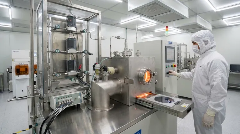
How CVD Builds a Microchip
CVD is one of the primary ways engineers construct the intricate, three-dimensional structures that make up transistors and the wiring that connects them.
The Fundamental Principle: Gas to Solid
The process begins by placing a silicon wafer inside a reaction chamber. One or more volatile precursor gases are then introduced.
These gases don't just coat the wafer. Instead, energy—typically in the form of heat—causes them to decompose and react on the wafer's surface, forming a stable, solid film and leaving behind volatile byproducts that are exhausted from the chamber.
This chemical transformation is what separates CVD from other techniques, allowing for the creation of high-purity, well-controlled material layers.
Key Materials Deposited by CVD
CVD is versatile and used to deposit the most critical materials in a chip.
- Insulators (Dielectrics): Silicon dioxide (SiO₂) and silicon nitride (Si₃N₄) are deposited to electrically isolate different components from one another.
- Conductors and Semiconductors: Polysilicon is a critical material for forming the "gate" of a transistor, which acts as a switch. CVD is also used to deposit metal films like tungsten that serve as electrical contacts.
- Complex Films: Advanced techniques like MOCVD are used to create compound semiconductors (e.g., for LEDs) and other highly engineered films where precise composition is critical.
A Guide to Key CVD Techniques
The term "CVD" encompasses several distinct methods, each optimized for a specific application or stage in the fabrication process.
LPCVD (Low-Pressure CVD)
LPCVD is performed at high temperatures and very low pressures. This combination results in films with excellent purity and uniformity across the entire wafer.
It is the preferred method for depositing high-quality silicon nitride and polysilicon layers where thermal budget is not a primary concern.
PECVD (Plasma-Enhanced CVD)
PECVD uses an electromagnetic field (plasma) to energize the precursor gases instead of relying solely on high temperature.
This allows deposition to occur at much lower temperatures, making it indispensable for depositing films on top of layers that would be damaged by the heat of an LPCVD process. It is a workhorse for depositing insulating films.
HDP-CVD (High-Density Plasma CVD)
As transistors shrink, the gaps between components become incredibly deep and narrow (high aspect ratio). Filling these gaps without creating voids is a major challenge.
HDP-CVD solves this by simultaneously depositing material and using ionized argon gas to sputter and etch it away. This dual-action process effectively fills tiny trenches from the bottom up, preventing the formation of voids that would otherwise cause device failure.
Understanding the Trade-offs
Selecting a deposition technology is never about finding the "best" one, but the right one for a specific task. The decision always involves balancing competing factors.
Temperature vs. Film Quality
Higher process temperatures, like those in LPCVD, generally produce higher-density, higher-purity films.
However, once temperature-sensitive metal layers have been fabricated on the chip, high-temperature processes can no longer be used. This forces engineers to use lower-temperature PECVD for subsequent layers, even if it means a slight compromise on film properties.
Speed vs. Precision
Some CVD processes are optimized for high-throughput manufacturing, rapidly depositing films to keep production moving.
Other techniques, like the related Atomic Layer Deposition (ALD), take this principle to its extreme. ALD deposits material one single atomic layer at a time, offering unparalleled thickness control and conformality at the cost of being a much slower process.
Conformality: The Ability to Cover Complex Shapes
Conformality refers to how well a deposited film conforms to the shape of the underlying topography. CVD processes generally offer superior conformality compared to Physical Vapor Deposition (PVD), which is more of a line-of-sight process.
For the most aggressive features, like the deep gaps in modern logic chips, a highly conformal process like HDP-CVD is not just preferred—it's essential.
Making the Right Choice for Your Goal
The right deposition strategy is dictated entirely by the specific material requirements and the constraints of the fabrication step.
- If your primary focus is creating high-purity, uniform base layers and temperature is not a constraint: LPCVD is the optimal choice for materials like polysilicon and silicon nitride.
- If your primary focus is depositing insulator films on temperature-sensitive underlying structures: PECVD provides the essential, reliable, lower-temperature solution.
- If your primary focus is filling deep, narrow trenches without creating device-killing voids: HDP-CVD is specifically engineered for this critical high-aspect-ratio gap-fill challenge.
- If your primary focus is depositing compound semiconductors or films with precise elemental composition: MOCVD offers the control needed for advanced materials used in optoelectronics and next-generation transistors.
Ultimately, mastering the art and science of chemical vapor deposition is fundamental to pushing the boundaries of what is possible in semiconductor technology.
Summary Table:
| CVD Technique | Primary Use Case | Key Advantage |
|---|---|---|
| LPCVD | High-purity base layers (e.g., polysilicon, silicon nitride) | Excellent film uniformity and purity at high temperatures |
| PECVD | Insulator films on temperature-sensitive structures | Lower-temperature deposition enabled by plasma |
| HDP-CVD | Filling deep, narrow trenches in advanced logic chips | Superior gap-fill capability without voids |
| MOCVD | Compound semiconductors and precise composition films | Control over complex material deposition |
Ready to optimize your semiconductor fabrication process? The right CVD equipment is critical for depositing high-quality insulating, conducting, and semiconducting layers. KINTEK specializes in providing advanced lab equipment and consumables tailored to your laboratory's semiconductor manufacturing needs.
Contact our experts today via our Contact Form to discuss how our solutions can enhance your film deposition quality, throughput, and yield.
Visual Guide

Related Products
- Chemical Vapor Deposition CVD Equipment System Chamber Slide PECVD Tube Furnace with Liquid Gasifier PECVD Machine
- Customer Made Versatile CVD Tube Furnace Chemical Vapor Deposition Chamber System Equipment
- Microwave Plasma Chemical Vapor Deposition MPCVD Machine System Reactor for Lab and Diamond Growth
- 915MHz MPCVD Diamond Machine Microwave Plasma Chemical Vapor Deposition System Reactor
- Custom CVD Diamond Coating for Lab Applications
People Also Ask
- What is the chemical vapor deposition growth process? Build Superior Thin Films from the Atom Up
- What are the advantages of chemical vapor deposition? Achieve Superior Thin Films for Your Lab
- How expensive is chemical vapor deposition? Understanding the True Cost of High-Performance Coating
- What is plasma enhanced chemical vapor deposition PECVD equipment? A Guide to Low-Temperature Thin Film Deposition
- Why is Chemical Vapor Deposition (CVD) equipment uniquely suited for constructing hierarchical superhydrophobic structures?


