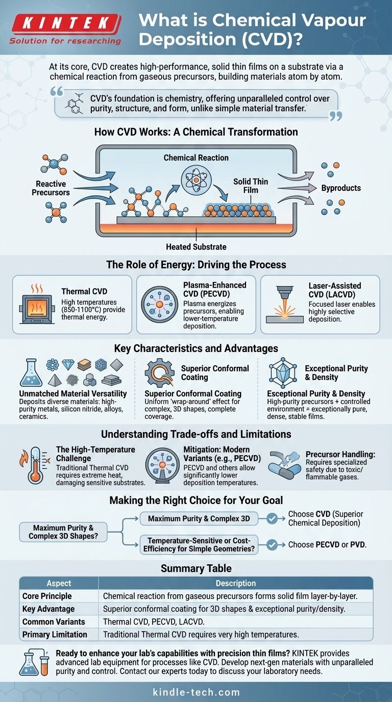
At its core, Chemical Vapor Deposition (CVD) is a process used to create high-performance, solid thin films on a surface, known as a substrate. It accomplishes this not by physical means, but by introducing reactive gases (precursors) into a chamber, which then undergo a chemical reaction at the substrate's surface to form the desired material layer by layer.
The critical difference between CVD and other coating methods is its foundation in chemistry. Instead of simply transferring a material from a source to a target, CVD builds a new material directly on the substrate from gaseous chemical ingredients, offering unparalleled control over purity, structure, and form.
How Chemical Vapor Deposition Works
CVD is a sophisticated manufacturing technique essential for producing materials used in electronics, optics, and protective coatings. The process can be broken down into a few key principles.
The Core Principle: A Chemical Transformation
The process begins by introducing one or more volatile gases, called precursors, into a reaction chamber containing the object to be coated (the substrate). Energy is then applied to the system. This energy breaks down the precursor gases and triggers a chemical reaction on the heated substrate surface, leaving behind a solid film of the desired material. The leftover gaseous byproducts are then vented out.
The Role of Energy
Energy is the catalyst that drives the entire CVD process. The type of energy used defines the specific variant of CVD and its ideal applications.
- Thermal CVD: This is the most common form, using high temperatures (often 850-1100°C) to provide the thermal energy needed for the chemical reaction.
- Plasma-Enhanced CVD (PECVD): This method uses a plasma (an ionized gas) to energize the precursors, allowing the deposition to occur at much lower temperatures.
- Laser-Assisted CVD (LACVD): A focused laser provides the energy, enabling highly selective deposition on specific areas of the substrate.
The Power of Control
By carefully adjusting process parameters like temperature, pressure, and the mix of precursor gases, engineers can precisely control the final film's characteristics. This includes its thickness, chemical composition, crystal structure, and grain size.
Key Characteristics and Advantages of CVD
The chemical nature of the CVD process gives it several distinct advantages over physical methods.
Unmatched Material Versatility
CVD can be used to deposit a vast array of materials that are often difficult to produce otherwise. This includes high-purity metals, non-metal films like silicon nitride, multi-component alloys, and advanced ceramic compounds.
Superior Conformal Coating
Because the deposition occurs from a gas phase, the material forms uniformly over all exposed surfaces of the substrate. This "wrap-around" effect is excellent for coating complex, three-dimensional shapes, ensuring complete coverage where physical, line-of-sight methods would fail.
Exceptional Purity and Density
The process starts with high-purity precursor gases, and the controlled reaction environment prevents the introduction of contaminants. The resulting films are exceptionally pure and dense, with very low residual stress, leading to a stable and high-quality crystalline structure.
Understanding the Trade-offs and Limitations
No technology is without its compromises. True expertise requires understanding both the strengths and weaknesses of a process.
The High-Temperature Challenge
A primary limitation of traditional thermal CVD is the extremely high temperature required. Many potential substrate materials, such as certain polymers or lower-melting-point metals, cannot withstand these conditions without being damaged or destroyed.
The Mitigation: Modern CVD Variants
To overcome the temperature barrier, processes like Plasma-Enhanced CVD (PECVD) were developed. By using a plasma to energize the reaction, deposition can occur at significantly lower temperatures, expanding the range of compatible substrates.
Precursor Handling and Cost
The precursor gases used in CVD can be highly toxic, flammable, or corrosive, requiring specialized handling procedures and safety equipment. This complexity, along with the need for vacuum systems, can increase the operational cost and complexity compared to simpler coating methods.
Making the Right Choice for Your Goal
Selecting the correct deposition technology depends entirely on the requirements of your final product.
- If your primary focus is maximum purity and coating complex 3D shapes: CVD's chemical, atom-by-atom deposition process is often the superior choice.
- If your primary focus is coating temperature-sensitive substrates or achieving cost-efficiency for simple geometries: A lower-temperature CVD variant like PECVD or an alternative like Physical Vapor Deposition (PVD) may be more appropriate.
Understanding this fundamental distinction between chemical creation and physical transfer is the key to leveraging the power of advanced material deposition.
Summary Table:
| Aspect | Description |
|---|---|
| Core Principle | A chemical reaction from gaseous precursors forms a solid thin film layer-by-layer on a substrate. |
| Key Advantage | Superior conformal coating for complex 3D shapes and exceptional material purity and density. |
| Common Variants | Thermal CVD, Plasma-Enhanced CVD (PECVD), Laser-Assisted CVD (LACVD). |
| Primary Limitation | Traditional thermal CVD requires very high temperatures, which can damage some substrates. |
Ready to enhance your lab's capabilities with precision thin films?
KINTEK specializes in providing the advanced lab equipment and consumables needed for sophisticated processes like Chemical Vapor Deposition. Whether you are developing next-generation electronics, optical coatings, or protective materials, our expertise can help you achieve unparalleled purity and control.
Contact our experts today to discuss how our solutions can meet your specific laboratory needs and drive your research forward.
Visual Guide
Related Products
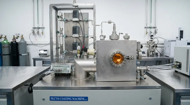
- Chemical Vapor Deposition CVD Equipment System Chamber Slide PECVD Tube Furnace with Liquid Gasifier PECVD Machine
- Customer Made Versatile CVD Tube Furnace Chemical Vapor Deposition Chamber System Equipment
- Microwave Plasma Chemical Vapor Deposition MPCVD Machine System Reactor for Lab and Diamond Growth
- 915MHz MPCVD Diamond Machine Microwave Plasma Chemical Vapor Deposition System Reactor
- Custom CVD Diamond Coating for Lab Applications
People Also Ask
- What are the advantages of chemical vapor deposition? Achieve Superior Thin Films for Your Lab
- What are the processes of vapor phase deposition? Understand CVD vs. PVD for Superior Thin Films
- What are the core advantages of PE-CVD in OLED encapsulation? Protect Sensitive Layers with Low-Temp Film Deposition
- How are carbon nanotubes grown? Master Scalable Production with Chemical Vapor Deposition
- What types of substrates are used in CVD to facilitate graphene films? Optimize Graphene Growth with the Right Catalyst


