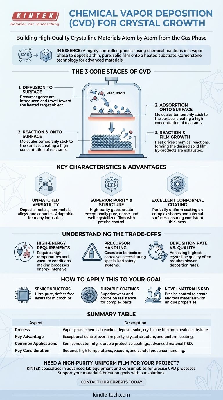
In essence, Chemical Vapor Deposition (CVD) is a highly controlled process for building high-quality, solid crystalline materials directly onto a surface from a gas. It involves introducing reactive gases into a chamber where they decompose and deposit a thin film, one layer of atoms at a time, onto a heated object known as a substrate.
The core principle behind CVD is using a chemical reaction in a vapor or gas phase to create a solid product. This method offers exceptional control over the final material's purity, structure, and thickness, making it a cornerstone technology for manufacturing advanced materials like semiconductors and durable coatings.
The Three Core Stages of CVD Explained
To understand how CVD achieves such precision, it's best to break it down into its three fundamental stages. The entire process occurs within a controlled-environment chamber.
Stage 1: Diffusion to the Surface
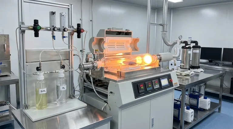
First, one or more reactive gases, known as precursors, are introduced into the reaction chamber. These gases then diffuse through the chamber and travel toward the target object, or substrate, which is typically heated to a specific temperature to drive the process.
Stage 2: Adsorption onto the Surface
Once the precursor gas molecules reach the substrate, they land and temporarily stick to its surface. This physical process, called adsorption, creates a high concentration of reactants exactly where the new material needs to grow.
Stage 3: Reaction and Film Growth
This is the critical step. The heat from the substrate provides the energy for the adsorbed gas molecules to chemically react. This reaction forms the desired solid material, which deposits onto the substrate as a thin film. Any leftover gaseous by-products are then released (desorbed) from the surface and are exhausted from the chamber.
Key Characteristics and Advantages of CVD
The reason CVD is so widely used is because of the superior qualities of the films it produces. It isn't just a simple coating method; it's a material fabrication technique.
Unmatched Versatility
CVD is not limited to one type of material. The process can be adapted to deposit a vast range of materials, including metals, non-metal films, complex alloys, and durable ceramics. This flexibility makes it invaluable across many industries.
Superior Purity and Structure
Because the process starts with high-purity gases in a controlled vacuum environment, the resulting films are exceptionally pure, dense, and well-crystallized. By carefully adjusting deposition parameters like temperature, pressure, and gas flow, engineers can precisely control the final film's crystal structure, grain size, and chemical composition.
Excellent Conformal Coating
One of CVD's most significant advantages is its ability to create a perfectly uniform coating, even on objects with complex shapes and internal surfaces. This "wrap-around" effect ensures that the film thickness is consistent everywhere, which is critical for protecting intricate parts or fabricating complex microelectronic devices.
Understanding the Trade-offs
While powerful, CVD is a sophisticated process with specific requirements and is not always the right solution for every application.
High-Energy Requirements
Most CVD processes require high temperatures and high-vacuum conditions to proceed correctly. This makes the equipment complex and the process itself can be energy-intensive compared to simpler coating methods like painting or electroplating.
Precursor Handling
The precursor gases used in CVD can often be toxic, flammable, or corrosive. This necessitates specialized handling procedures, safety systems, and infrastructure, which adds to the overall cost and complexity of the operation.
Deposition Rate vs. Quality
The exceptional control offered by CVD can sometimes come at the cost of speed. While some CVD techniques are fast, achieving the highest levels of crystalline perfection and uniformity often requires slower deposition rates.
How to Apply This to Your Goal
Choosing CVD depends entirely on the required performance and quality of the final product.
- If your primary focus is producing high-performance semiconductors: CVD is essential for its ability to grow the ultra-pure, defect-free crystalline layers required for microchips.
- If your primary focus is enhancing the durability of complex mechanical parts: The dense, conformal coatings from CVD provide superior wear and corrosion resistance for components like turbine blades or cutting tools.
- If your primary focus is research and development of novel materials: CVD offers the precise control over composition and structure needed to create and test materials with unique electronic, optical, or physical properties.
Ultimately, Chemical Vapor Deposition gives us the power to construct advanced materials from the atom up, enabling the technology that defines our modern world.
Summary Table:
| Aspect | Description |
|---|---|
| Process | Vapor-phase chemical reaction deposits a solid, crystalline film onto a heated substrate. |
| Key Advantage | Exceptional control over film purity, crystal structure, and uniform, conformal coating. |
| Common Applications | Semiconductor manufacturing, durable protective coatings, advanced material R&D. |
| Key Consideration | Requires high temperatures, vacuum conditions, and careful handling of precursor gases. |
Need to deposit a high-purity, uniform film for your project?
KINTEK specializes in providing the advanced lab equipment and consumables required for precise Chemical Vapor Deposition processes. Whether you are developing next-generation semiconductors, creating durable coatings for complex components, or pushing the boundaries of material science, our solutions support the high-quality results that CVD is known for.
Contact our experts today to discuss how we can help you achieve your material fabrication goals.
Visual Guide
Related Products
- Chemical Vapor Deposition CVD Equipment System Chamber Slide PECVD Tube Furnace with Liquid Gasifier PECVD Machine
- Microwave Plasma Chemical Vapor Deposition MPCVD Machine System Reactor for Lab and Diamond Growth
- 915MHz MPCVD Diamond Machine Microwave Plasma Chemical Vapor Deposition System Reactor
- Customer Made Versatile CVD Tube Furnace Chemical Vapor Deposition Chamber System Equipment
- Split Chamber CVD Tube Furnace with Vacuum Station Chemical Vapor Deposition System Equipment Machine
People Also Ask
- What are the core advantages of PE-CVD in OLED encapsulation? Protect Sensitive Layers with Low-Temp Film Deposition
- How expensive is chemical vapor deposition? Understanding the True Cost of High-Performance Coating
- What types of substrates are used in CVD to facilitate graphene films? Optimize Graphene Growth with the Right Catalyst
- What is the chemical vapor deposition growth process? Build Superior Thin Films from the Atom Up
- Why is Chemical Vapor Deposition (CVD) equipment uniquely suited for constructing hierarchical superhydrophobic structures?


