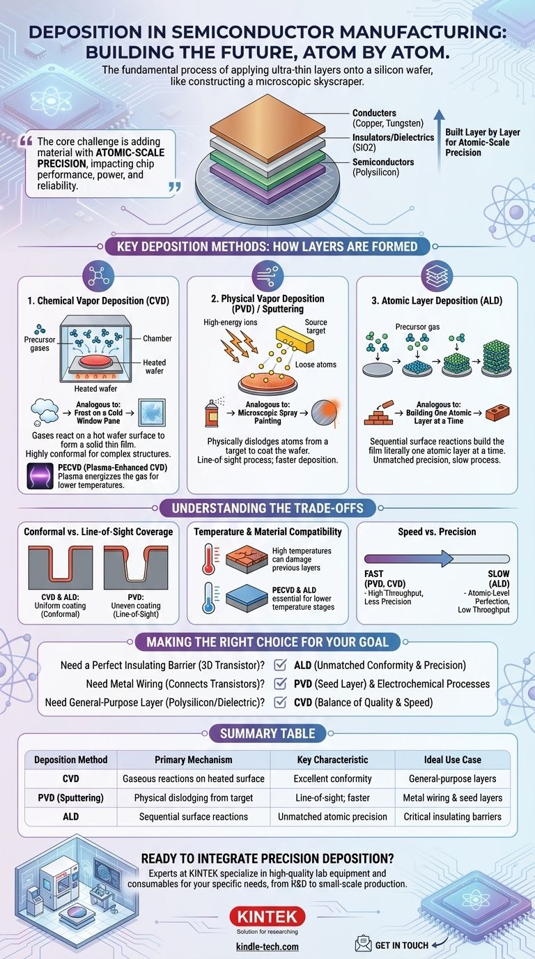
In semiconductor manufacturing, deposition is the fundamental process of applying ultra-thin layers of material onto a silicon wafer. Think of it as constructing a microscopic skyscraper, where each "floor" is a precisely engineered film that serves a specific electrical purpose. These layers, often just a few atoms thick, are the essential building blocks for creating transistors, interconnects, and the other components that form a complete integrated circuit.
The core challenge of deposition is not simply adding material, but doing so with atomic-scale precision. The choice of deposition method is a critical engineering decision that directly impacts a chip's performance, power consumption, and reliability.
The Core Function: Building a Chip Layer by Layer
Modern microchips are not carved from a single block of silicon. Instead, they are built upwards through the repeated application of patterned layers, with deposition being the key process for adding each new layer of material.
What is a Thin Film?
A "thin film" is a layer of material ranging from a few nanometers to several micrometers in thickness. In chip fabrication, these films are generally one of three types: conductors (like copper or tungsten for wiring), insulators or dielectrics (like silicon dioxide to prevent short circuits), and semiconductors (like polysilicon for transistor gates).
The Goal: Absolute Precision and Purity
The function of each circuit depends on the perfect thickness, uniformity, and chemical purity of these deposited films. Even a minuscule variation or a single contaminant particle across the wafer can render millions of transistors useless, destroying the entire chip.
Key Deposition Methods: How Layers Are Formed
While dozens of deposition techniques exist, they primarily fall into a few key families, each with a distinct physical mechanism. The method chosen depends entirely on the material being deposited and its role in the final device.
Chemical Vapor Deposition (CVD)
CVD involves introducing precursor gases into a reaction chamber where the wafer is heated. These gases react on the wafer's hot surface, forming a solid thin film and leaving behind gaseous byproducts that are vented away. It's conceptually similar to how steam condenses into a uniform layer of frost on a cold window pane.
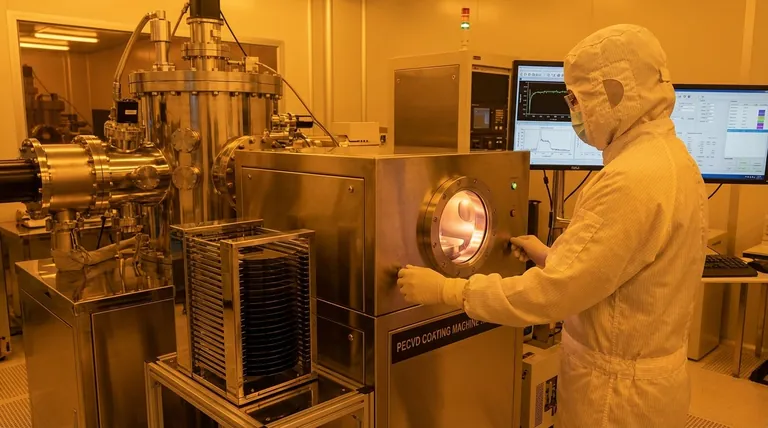
Common variations like Plasma-Enhanced CVD (PECVD) use plasma to energize the gas, allowing the reaction to occur at much lower temperatures. This is crucial for preventing damage to layers that have already been built on the wafer.
Physical Vapor Deposition (PVD)
PVD, also known as sputtering, works by physically dislodging atoms from a source material (called a "target"). In a vacuum chamber, the target is bombarded with high-energy ions, knocking atoms loose. These liberated atoms then travel through the vacuum and coat the wafer.
This process is best understood as a form of microscopic spray painting, where individual atoms are the "paint" being sprayed onto the wafer's surface.
Atomic Layer Deposition (ALD)
ALD is the most precise method available, building the film literally one atomic layer at a time. It uses a sequence of self-limiting chemical reactions, where precursor gases are pulsed into the chamber one after another. Each pulse adds exactly one monolayer of atoms.
While much slower than other methods, ALD provides unparalleled control over thickness and ensures the film perfectly conforms to even the most complex, three-dimensional microscopic structures.
Understanding the Trade-offs
The existence of so many deposition methods highlights a core engineering truth: there is no single "best" technique. Each involves critical trade-offs between speed, material quality, and the ability to cover complex topologies.
Conformal vs. Line-of-Sight Coverage
One of the most important distinctions is how a method handles 3D structures. CVD and ALD are highly conformal, meaning they can deposit a perfectly uniform layer over complex, non-flat surfaces, like the inside of a deep trench.
In contrast, PVD is a line-of-sight process. Like a spray can, it can only coat the surfaces it can "see," often resulting in thicker material at the top of a trench and much thinner material at the bottom.
Temperature and Material Compatibility
High temperatures can be destructive. The heat required for some CVD processes can damage previously deposited layers or cause materials to diffuse into one another, ruining their electrical properties. This is why lower-temperature methods like PECVD and ALD are essential for later stages of chip fabrication.
Speed vs. Precision
There is an unavoidable trade-off between manufacturing speed (throughput) and film quality. Processes like ALD offer atomic-level perfection but are very slow. For thicker, less critical layers where such precision isn't needed, a faster CVD or PVD process is far more economical.
Making the Right Choice for Your Goal
The selection of a deposition technique is always driven by the specific requirements of the layer being built.
- If your primary focus is creating a perfect, pinhole-free insulating barrier in a 3D transistor: ALD is the only choice for its unmatched conformity and precision at the atomic scale.
- If your primary focus is depositing the metal wiring that connects transistors: A combination of PVD (to create an initial "seed" layer) and other electrochemical processes is the industry standard.
- If your primary focus is depositing a general-purpose polysilicon or dielectric layer: A form of CVD often provides the ideal balance of film quality, conformity, and manufacturing speed.
Ultimately, mastering deposition is about selecting the ideal tool to construct each specific, nanometer-scale layer of a modern integrated circuit.
Summary Table:
| Deposition Method | Primary Mechanism | Key Characteristic | Ideal Use Case |
|---|---|---|---|
| Chemical Vapor Deposition (CVD) | Gaseous chemical reactions on a heated wafer surface. | Excellent conformity over complex 3D structures. | General-purpose dielectric and semiconductor layers. |
| Physical Vapor Deposition (PVD / Sputtering) | Physical dislodging of atoms from a target material. | Line-of-sight coverage; faster deposition. | Metal wiring and seed layers. |
| Atomic Layer Deposition (ALD) | Self-limiting, sequential surface chemical reactions. | Unmatched atomic-scale precision and conformity. | Critical insulating barriers in advanced 3D transistors. |
Ready to Integrate Precision Deposition into Your Lab Workflow?
Selecting the right deposition technique is critical for the performance of your semiconductor research or device fabrication. The experts at KINTEK specialize in providing high-quality lab equipment and consumables tailored to your specific deposition needs.
We understand the challenges of achieving atomic-scale precision and can help you select the ideal solution, whether your focus is on R&D, process development, or small-scale production.
Contact us today to discuss how our solutions can enhance your laboratory's capabilities and drive your projects forward.
Visual Guide
Related Products
- RF PECVD System Radio Frequency Plasma-Enhanced Chemical Vapor Deposition RF PECVD
- Evaporation Boat for Organic Matter
- Thin-Layer Spectral Electrolysis Electrochemical Cell
- Side Window Optical Electrolytic Electrochemical Cell
- Reference Electrode Calomel Silver Chloride Mercury Sulfate for Laboratory Use
People Also Ask
- Why is a Matching Network Indispensable in RF-PECVD for Siloxane Films? Ensure Stable Plasma and Uniform Deposition
- What is an example of PECVD? RF-PECVD for High-Quality Thin Film Deposition
- What is plasma enhanced chemical vapour deposition process? Unlock Low-Temperature, High-Quality Thin Films
- What is plasma enhanced chemical Vapour deposition process used for fabrication of? A Guide to Low-Temperature Thin Films
- What is plasma chemical vapor deposition? A Low-Temperature Thin Film Coating Solution


