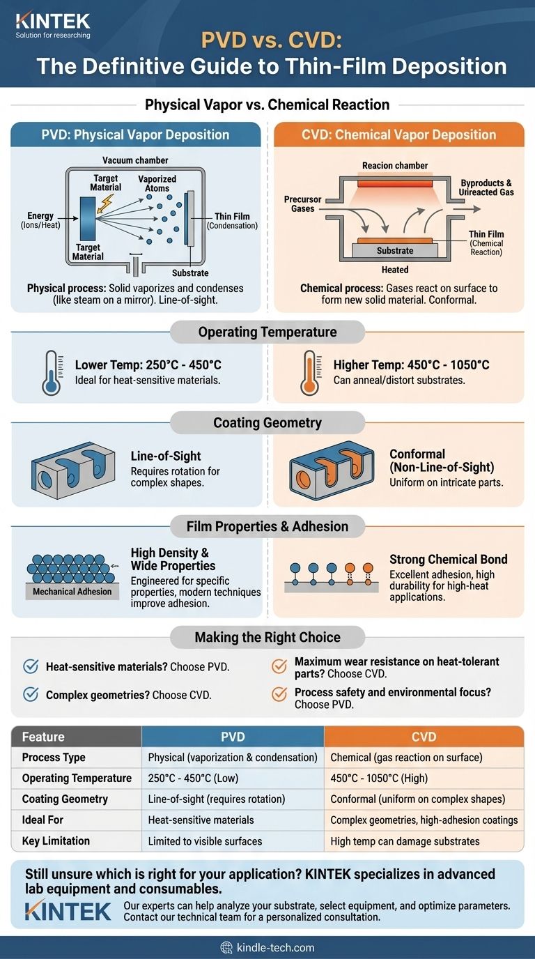
Fundamentally, the difference between PVD and CVD lies in how the thin film is created. Physical Vapor Deposition (PVD) is a physical process where a solid material is vaporized and then condenses onto the part's surface, much like steam fogging a cold mirror. Chemical Vapor Deposition (CVD), in contrast, is a chemical process where precursor gases react on the surface to form an entirely new solid material, the coating itself.
The choice between PVD and CVD is not about which is "better," but which is appropriate for the task. The core distinction—physical condensation versus chemical reaction—dictates critical factors like operating temperature and the ability to coat complex shapes, making the decision a function of your material and geometry.
The Core Process: Physical vs. Chemical
The names themselves reveal the primary distinction. One process relies on physics (changes in state), while the other relies on chemistry (formation of new substances).
PVD: A Physical Condensation Process
In PVD, the coating material starts as a solid target in a vacuum chamber. This solid is bombarded with energy (like ions in sputtering or heat in evaporation) that ejects atoms or molecules from its surface.
These vaporized particles travel in a straight line through the vacuum and deposit onto the substrate, physically building up the film layer by layer. No chemical reaction occurs on the substrate; it is a direct transfer of material from source to surface.
CVD: A Chemical Reaction on the Surface
In CVD, the substrate is placed in a reaction chamber and heated. A carefully controlled mix of precursor gases is then introduced.
When these gases come into contact with the hot substrate, they trigger a chemical reaction. This reaction decomposes the gases and forms a new, solid film on the surface of the part. The unreacted gases and byproducts are then pumped out.
How This Difference Impacts Your Application
The distinction between a physical and chemical process is not merely academic. It has direct, practical consequences for temperature, geometry, and film properties.
Operating Temperature
PVD operates at significantly lower temperatures, typically between 250°C and 450°C. This makes it ideal for coating materials that cannot withstand high heat without changing their fundamental properties.
CVD requires much higher temperatures to drive the necessary chemical reactions, usually between 450°C and 1050°C. This high heat can anneal, soften, or distort heat-sensitive substrates like tempered steel or aluminum alloys.
Coating Geometry (Line-of-Sight vs. Conformal)
PVD is a line-of-sight process. The vaporized coating material travels in a straight line, meaning it can only coat surfaces it can "see" from the source. Coating complex shapes or internal bores requires complex fixturing and part rotation to ensure even coverage.
CVD is a conformal (non-line-of-sight) process. Because the coating is formed from gases that flow around the part, it can uniformly coat intricate shapes, sharp edges, and even internal channels with ease.
Film Properties and Adhesion
CVD coatings often exhibit very strong adhesion because the film is chemically bonded to the substrate material. The high temperature promotes diffusion at the interface, creating a very durable link.
PVD coatings can be engineered to have extremely high density and a wide range of properties. While adhesion is typically mechanical, modern PVD techniques like high-power impulse magnetron sputtering (HiPIMS) can create exceptionally well-adhered films.
Understanding the Trade-offs
Neither technology is a universal solution. Choosing the right one requires acknowledging their inherent limitations.
The Heat Limitation of CVD
The primary drawback of traditional CVD is its high processing temperature. This immediately disqualifies it for a vast range of applications involving components that have already been heat-treated to achieve specific hardness or toughness.
The Geometric Limitation of PVD
The line-of-sight nature of PVD is its biggest challenge. Failing to account for this can lead to uneven or non-existent coatings on certain areas of a complex part, compromising its performance. Achieving uniformity often adds cost and complexity to the process.
Environmental and Safety Concerns
CVD processes frequently use precursor gases that are toxic, flammable, or corrosive. This necessitates significant investment in safety protocols, gas handling systems, and waste abatement, which can make it a more complex and hazardous operation than PVD. PVD, being a physical process in a vacuum, is generally considered more environmentally friendly.
Making the Right Choice for Your Application
Your decision should be guided by the non-negotiable requirements of your substrate and final part performance.
- If your primary focus is coating heat-sensitive materials (like tempered steel or aluminum): PVD is the correct choice due to its significantly lower operating temperature.
- If your primary focus is creating a uniform coating on parts with complex internal geometries: CVD is superior because the precursor gases can penetrate and react on all exposed surfaces.
- If your primary focus is maximum wear resistance on a substrate that can tolerate high heat: CVD often provides exceptional adhesion and film quality, making it a leading choice for applications like carbide cutting tools.
- If your primary focus is process safety and environmental impact: PVD is generally the simpler and "greener" technology, avoiding the hazardous gases common to many CVD processes.
By understanding the fundamental trade-off between PVD's physical deposition and CVD's chemical reaction, you can confidently select the right technology for your specific engineering goal.
Summary Table:
| Feature | PVD (Physical Vapor Deposition) | CVD (Chemical Vapor Deposition) |
|---|---|---|
| Process Type | Physical (vaporization & condensation) | Chemical (gas reaction on surface) |
| Operating Temperature | 250°C - 450°C (Low) | 450°C - 1050°C (High) |
| Coating Geometry | Line-of-sight (requires rotation for complex shapes) | Conformal (uniform on complex shapes & internal channels) |
| Ideal For | Heat-sensitive materials (tempered steel, aluminum) | Complex geometries, high-adhesion coatings on heat-tolerant substrates |
| Key Limitation | Limited to surfaces visible from the source | High temperature can damage heat-sensitive substrates |
Still unsure whether PVD or CVD is right for your specific application?
KINTEK specializes in providing advanced lab equipment and consumables for thin-film deposition, serving a wide range of laboratory needs. Our experts can help you:
- Analyze your substrate material and geometry to determine the optimal coating process
- Select the right equipment for your specific PVD or CVD requirements
- Optimize your coating parameters for superior film quality and performance
Don't leave your coating results to chance—contact our technical team today for a personalized consultation and ensure you choose the right technology for your project's success!
Visual Guide
Related Products
- Inclined Rotary Plasma Enhanced Chemical Vapor Deposition PECVD Equipment Tube Furnace Machine
- HFCVD Machine System Equipment for Drawing Die Nano-Diamond Coating
- 915MHz MPCVD Diamond Machine Microwave Plasma Chemical Vapor Deposition System Reactor
- Vacuum Hot Press Furnace Machine for Lamination and Heating
- Laboratory CVD Boron Doped Diamond Materials
People Also Ask
- How does plasma enhanced CVD work? Achieve Low-Temperature, High-Quality Thin Film Deposition
- What is PECVD used for? Achieve Low-Temperature, High-Performance Thin Films
- What materials are deposited in PECVD? Discover the Versatile Thin-Film Materials for Your Application
- What is the difference between CVD and PECVD? Choose the Right Thin-Film Deposition Method
- What is PECVD silicon deposition? Achieve Low-Temperature, High-Quality Thin Films


