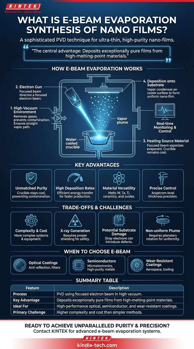
At its core, electron beam evaporation is a sophisticated technique for creating ultra-thin, high-purity films with nanometer-scale thickness. It is a form of physical vapor deposition (PVD) where a powerful, focused beam of electrons bombards a source material inside a high-vacuum chamber. This intense energy vaporizes the material, which then travels and condenses onto a cooler surface (the substrate), forming a uniform nano-film.
The central advantage of e-beam evaporation is its ability to deposit exceptionally pure films from materials with very high melting points, offering a level of control and quality that simpler methods cannot achieve.
How E-Beam Evaporation Works: A Step-by-Step Breakdown
Understanding the process reveals why this technique is so powerful for advanced material synthesis. The entire operation takes place inside a high-vacuum chamber to ensure the purity of the final film.
The High-Vacuum Environment
First, the chamber is pumped down to a very low pressure. This high vacuum is critical because it removes residual gas molecules, like oxygen and water vapor, that could otherwise contaminate the film. It also ensures the vaporized atoms can travel directly to the substrate without colliding with other particles.
The Electron Gun
The heart of the system is the electron gun, which typically uses a heated tungsten filament to generate a stream of electrons. These electrons are then accelerated by high voltage and focused into a tight beam using magnetic fields, much like in an old cathode-ray tube television.
Heating the Source Material
This high-energy electron beam is directed onto the source material, or evaporant, which is held in a water-cooled copper hearth or crucible. The beam's kinetic energy is converted to thermal energy upon impact, rapidly heating a small spot on the material to its boiling point and causing it to vaporize.
Deposition onto the Substrate
The vaporized atoms travel in a straight line from the source to the target substrate (such as a silicon wafer or glass slide) positioned above. Upon reaching the cooler substrate, the atoms condense and begin to form a thin, solid film. The thickness is monitored in real-time, often with a quartz crystal microbalance, allowing for precise control.
Key Advantages of the E-Beam Method
Engineers and scientists choose this method for several distinct benefits that set it apart from other deposition techniques like thermal evaporation or sputtering.
Unmatched Purity
Because the electron beam heats only the surface of the source material, the crucible itself remains cool. This prevents contamination from the crucible material melting or outgassing, which can be a significant issue in simpler thermal evaporation systems.
High Deposition Rates
E-beam systems transfer energy to the source material very efficiently. This allows for much higher deposition rates compared to many other techniques, making it suitable for both research and industrial-scale production.
Versatility with Materials
The intense, localized heating can melt and vaporize materials with extremely high melting points, such as tungsten, tantalum, and titanium, as well as various ceramics and oxides. This is a capability that resistive thermal evaporation simply cannot match.
Precise Control Over Film Thickness
The combination of a stable evaporation rate and real-time monitoring allows for the creation of films with angstrom-level precision. This is essential for creating complex structures like optical filters or semiconductor devices.
Understanding the Trade-offs and Challenges
While powerful, e-beam evaporation is not without its complexities and potential downsides. An objective assessment requires acknowledging these factors.
Equipment Complexity and Cost
E-beam systems are significantly more complex and expensive than basic thermal evaporators. They require high-voltage power supplies, sophisticated magnetic focusing systems, and robust vacuum pumps.
Generation of X-rays
The high-energy electrons striking the source material inevitably generate X-rays. This requires proper shielding of the vacuum chamber to ensure operator safety, adding to the system's cost and complexity.
Potential for Substrate Damage
Stray electrons or ionized vapor atoms can sometimes bombard the substrate, potentially causing damage or introducing defects into the growing film. Careful system design is required to mitigate this risk.
Non-uniform Vapor Plume
The vapor stream from the source is not perfectly uniform. To achieve a film of even thickness across a large substrate, a planetary rotation system is often necessary to continually change the substrate's orientation relative to the source.
When to Choose E-Beam Evaporation
Your choice of deposition method should be driven by the specific requirements of your application and material.
- If your primary focus is high-performance optical coatings: E-beam is the industry standard, providing the dense, pure, and precisely layered films required for anti-reflection coatings and filters.
- If your primary focus is advanced semiconductors or microelectronics: The ability to deposit high-purity refractory metals and oxides with great precision makes this technique essential.
- If your primary focus is wear-resistant or thermal barrier coatings: E-beam is frequently used in the aerospace and tooling industries to deposit durable ceramic films.
- If your primary focus is simple metal contacts on a limited budget: A less complex method like thermal evaporation or sputtering may be a more practical and cost-effective choice.
Ultimately, selecting e-beam evaporation is a decision to prioritize film purity, material versatility, and precise control over equipment simplicity and cost.
Summary Table:
| Feature | Description |
|---|---|
| Process | Physical Vapor Deposition (PVD) using a focused electron beam in a high vacuum. |
| Key Advantage | Deposits exceptionally pure films from materials with very high melting points. |
| Ideal For | High-performance optical coatings, advanced semiconductors, wear-resistant coatings. |
| Primary Challenge | Higher equipment complexity and cost compared to simpler methods like thermal evaporation. |
Ready to achieve unparalleled purity and precision in your thin-film deposition?
At KINTEK, we specialize in providing advanced lab equipment, including sophisticated e-beam evaporation systems, to meet the demanding needs of semiconductor, optical coating, and materials science laboratories. Our solutions are designed to deliver the high-purity, high-melting-point material deposition your research and production require.
Contact our experts today via our Contact Form to discuss how our e-beam evaporation technology can enhance your capabilities and drive your innovations forward.
Visual Guide
Related Products
- Electron Beam Evaporation Coating Oxygen-Free Copper Crucible and Evaporation Boat
- Electron Beam Evaporation Coating Tungsten Crucible and Molybdenum Crucible for High Temperature Applications
- Electron Beam Evaporation Coating Gold Plating Tungsten Molybdenum Crucible for Evaporation
- E Beam Crucibles Electron Gun Beam Crucible for Evaporation
- Electron Beam Evaporation Coating Conductive Boron Nitride Crucible BN Crucible
People Also Ask
- What is the container that holds the metal source material called in e-beam evaporation? Ensure Purity and Quality in Your Thin-Film Deposition
- How is an electron beam evaporator cooled during deposition? Essential Thermal Management for Stable Processes
- What is the temperature of e-beam evaporation? Mastering the Two-Zone Thermal Process for Precision Films
- What is the deposition rate of e-beam evaporation? Control Thin Film Quality and Speed
- What is the voltage of e-beam evaporation? Achieve Precise Thin-Film Deposition


