Knowledge What is film thickness uniformity? Achieve Consistent Performance and Higher Yield
Author avatar

Tech Team · Kintek Solution

Updated 3 weeks ago

What is film thickness uniformity? Achieve Consistent Performance and Higher Yield

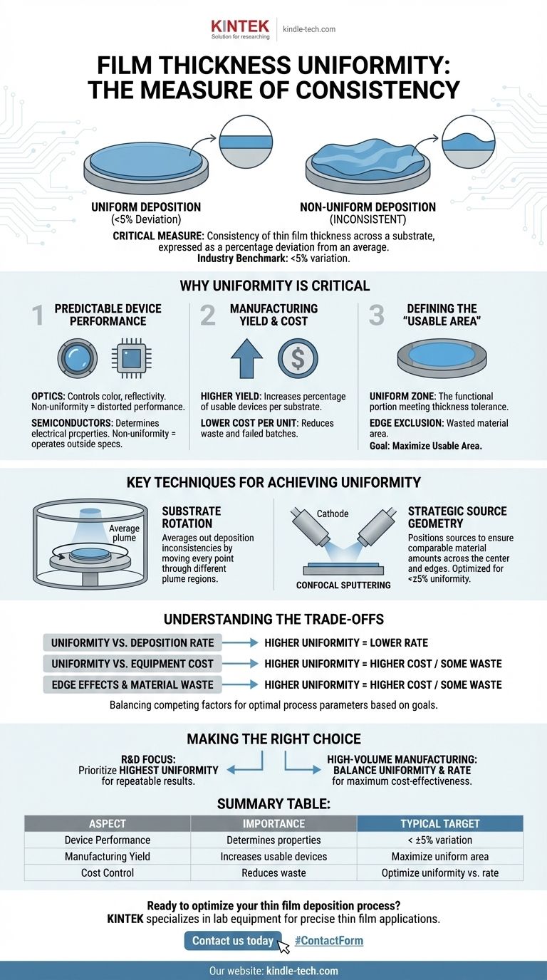
At its core, film thickness uniformity is a critical measure of how consistent the thickness of a deposited thin film is across the surface of a substrate. This consistency is not absolute; it is typically expressed as a percentage deviation from an average thickness. For example, a common industry benchmark for a "uniform area" is one where the film's thickness varies by less than 5% from the average value across that specific zone.

Film thickness uniformity is not merely a geometric property; it is a direct predictor of a device's functional performance and manufacturing yield. The goal is to control the deposition process so that every critical area of a substrate receives a nearly identical amount of material, ensuring predictable and reliable outcomes.

What is film thickness uniformity? Achieve Consistent Performance and Higher Yield

Why Uniformity is a Critical Metric

Achieving a specific thickness is only half the battle. Ensuring that thickness is consistent across the entire functional area of a substrate is what determines success or failure in many applications.

Predictable Device Performance

Slight variations in thickness can cause significant changes in a material's physical properties.

In optics, film thickness directly controls properties like color, reflectivity, and anti-reflection. A non-uniform coating on a lens will result in distorted optical performance.

In semiconductors, the thickness of gate oxides, conductors, and dielectric layers determines electrical characteristics like capacitance and resistance. Non-uniformity leads to devices that operate outside of their required specifications.

Manufacturing Yield and Cost

Every substrate that fails to meet thickness uniformity standards is a loss of time, materials, and money.

High uniformity translates directly to high manufacturing yield—the percentage of usable devices produced from a single substrate or batch. Increasing uniformity from 90% to 95% across a substrate can mean a significant increase in the number of viable chips or components, drastically lowering the cost per unit.

Defining the "Usable Area"

The "uniform area" is the portion of the substrate where the film meets the required thickness tolerance.

For practical purposes, this is the only part of the substrate that can be used to fabricate functional devices. The goal of process engineering is to maximize this usable area, pushing the uniform zone as close to the physical edge of the substrate as possible.

Key Techniques for Achieving Uniformity

Engineers use several well-established methods to control the deposition process and create highly uniform films. These techniques are designed to average out the natural inconsistencies of a deposition source.

Substrate Rotation

This is the most common and effective method for improving uniformity. By rotating the substrate during deposition, you ensure that every point on its surface passes through different regions of the deposition plume.

This movement averages out any "hot spots" or areas of lower flux from the source, resulting in a much more even coating than would be possible with a static substrate.

Strategic Source Geometry

The positioning of the deposition source relative to the substrate is critical. In processes like confocal sputtering, cathodes are intentionally tilted at an angle.

This, combined with substrate rotation, ensures that both the center and the outer edges of the substrate receive a comparable amount of deposited material over the course of the process. The exact tilt angle and target-to-substrate distance are carefully optimized to achieve uniformity often better than ±5%.

Understanding the Trade-offs

Pursuing perfect uniformity often involves balancing competing factors. There is no single "best" setup for all applications; there are only optimal solutions for specific goals.

Uniformity vs. Deposition Rate

Techniques that improve uniformity, such as increasing the distance between the source and the substrate, often reduce the deposition rate. This means the process takes longer, lowering throughput. A key engineering challenge is to find the sweet spot that provides acceptable uniformity without making the process time prohibitively long.

Uniformity vs. Equipment Cost

Achieving the highest levels of uniformity requires sophisticated equipment. Systems with planetary rotation, multiple sources, or complex magnetic field shaping are significantly more expensive to purchase and maintain than simpler, static systems. The required level of uniformity must justify the capital investment.

Edge Effects and Material Waste

It is nearly impossible to achieve perfect uniformity all the way to the physical edge of a substrate. This "edge exclusion" zone results in some wasted material and unusable substrate area. Minimizing this effect is a constant focus, but it can rarely be eliminated entirely.

Making the Right Choice for Your Process

Your approach to film thickness uniformity should be dictated by your end goal. Whether you prioritize absolute precision or manufacturing efficiency will determine your optimal process parameters.

  • If your primary focus is research and development: Prioritize achieving the highest possible uniformity to ensure your experimental results are repeatable and that material properties are the only changing variable.
  • If your primary focus is high-volume manufacturing: Aim for the most cost-effective balance between uniformity (to maximize device yield) and deposition rate (to maximize throughput).

Ultimately, mastering film thickness uniformity is about taking direct control over the quality and performance of your final product.

Summary Table:

Aspect Importance Typical Target
Device Performance Determines electrical/optical properties < ±5% variation
Manufacturing Yield Increases usable devices per substrate Maximize uniform area
Cost Control Reduces material waste and failed batches Optimize uniformity vs. rate

Ready to optimize your thin film deposition process? KINTEK specializes in lab equipment and consumables for precise thin film applications. Our expertise helps laboratories achieve superior film thickness uniformity, ensuring predictable device performance and higher manufacturing yields. Contact us today to discuss how our solutions can enhance your research or production efficiency!

Related Products

People Also Ask

Related Products

Inclined Rotary Plasma Enhanced Chemical Vapor Deposition PECVD Equipment Tube Furnace Machine

Inclined Rotary Plasma Enhanced Chemical Vapor Deposition PECVD Equipment Tube Furnace Machine

Upgrade your coating process with PECVD coating equipment. Ideal for LED, power semiconductors, MEMS and more. Deposits high-quality solid films at low temps.

HFCVD Machine System Equipment for Drawing Die Nano-Diamond Coating

HFCVD Machine System Equipment for Drawing Die Nano-Diamond Coating

The nano-diamond composite coating drawing die uses cemented carbide (WC-Co) as the substrate, and uses the chemical vapor phase method ( CVD method for short ) to coat the conventional diamond and nano-diamond composite coating on the surface of the inner hole of the mold.

915MHz MPCVD Diamond Machine Microwave Plasma Chemical Vapor Deposition System Reactor

915MHz MPCVD Diamond Machine Microwave Plasma Chemical Vapor Deposition System Reactor

915MHz MPCVD Diamond Machine and its multi-crystal effective growth, the maximum area can reach 8 inches, the maximum effective growth area of single crystal can reach 5 inches. This equipment is mainly used for the production of large-size polycrystalline diamond films, the growth of long single crystal diamonds, the low-temperature growth of high-quality graphene, and other materials that require energy provided by microwave plasma for growth.

Vacuum Hot Press Furnace Machine for Lamination and Heating

Vacuum Hot Press Furnace Machine for Lamination and Heating

Experience clean and precise lamination with Vacuum Lamination Press. Perfect for wafer bonding, thin-film transformations, and LCP lamination. Order now!

Small Vacuum Heat Treat and Tungsten Wire Sintering Furnace

Small Vacuum Heat Treat and Tungsten Wire Sintering Furnace

The small vacuum tungsten wire sintering furnace is a compact experimental vacuum furnace specially designed for universities and scientific research institutes. The furnace features a CNC welded shell and vacuum piping to ensure leak-free operation. Quick-connect electrical connections facilitate relocation and debugging, and the standard electrical control cabinet is safe and convenient to operate.

Graphite Vacuum Furnace IGBT Experimental Graphitization Furnace

Graphite Vacuum Furnace IGBT Experimental Graphitization Furnace

IGBT experimental graphitization furnace, a tailored solution for universities and research institutions, with high heating efficiency, user-friendliness, and precise temperature control.

Vacuum Heat Treat and Molybdenum Wire Sintering Furnace for Vacuum Sintering

Vacuum Heat Treat and Molybdenum Wire Sintering Furnace for Vacuum Sintering

A vacuum molybdenum wire sintering furnace is a vertical or bedroom structure, which is suitable for withdrawal, brazing, sintering and degassing of metal materials under high vacuum and high temperature conditions. It is also suitable for dehydroxylation treatment of quartz materials.

Molybdenum Vacuum Heat Treat Furnace

Molybdenum Vacuum Heat Treat Furnace

Discover the benefits of a high-configuration molybdenum vacuum furnace with heat shield insulation. Ideal for high-purity, vacuum environments like sapphire crystal growth and heat treatment.

1400℃ Laboratory Quartz Tube Furnace with Alumina Tube Tubular Furnace

1400℃ Laboratory Quartz Tube Furnace with Alumina Tube Tubular Furnace

Looking for a tube furnace for high-temperature applications? Our 1400℃ Tube Furnace with Alumina Tube is perfect for research and industrial use.

Vacuum Dental Porcelain Sintering Furnace

Vacuum Dental Porcelain Sintering Furnace

Get precise and reliable results with KinTek's Vacuum Porcelain Furnace. Suitable for all porcelain powders, it features hyperbolic ceramic furnace function, voice prompt, and automatic temperature calibration.

Laboratory Quartz Tube Furnace Tubular RTP Heating Furnace

Laboratory Quartz Tube Furnace Tubular RTP Heating Furnace

Get lightning-fast heating with our RTP Rapid Heating Tube Furnace. Designed for precise, high-speed heating and cooling with convenient sliding rail and TFT touch screen controller. Order now for ideal thermal processing!

Laboratory Vacuum Tilt Rotary Tube Furnace Rotating Tube Furnace

Laboratory Vacuum Tilt Rotary Tube Furnace Rotating Tube Furnace

Discover the versatility of Laboratory Rotary Furnace: Ideal for calcination, drying, sintering, and high-temperature reactions. Adjustable rotating and tilting functions for optimal heating. Suitable for vacuum and controlled atmosphere environments. Learn more now!

1700℃ Muffle Oven Furnace for Laboratory

1700℃ Muffle Oven Furnace for Laboratory

Get superior heat control with our 1700℃ Muffle Furnace. Equipped with intelligent temperature microprocessor, TFT touch screen controller & advanced insulation materials for precise heating up to 1700C. Order now!

Vacuum Sealed Continuous Working Rotary Tube Furnace Rotating Tube Furnace

Vacuum Sealed Continuous Working Rotary Tube Furnace Rotating Tube Furnace

Experience efficient material processing with our vacuum-sealed rotary tube furnace. Perfect for experiments or industrial production, equipped with optional features for controlled feeding and optimized results. Order now.

Graphite Vacuum Furnace High Thermal Conductivity Film Graphitization Furnace

Graphite Vacuum Furnace High Thermal Conductivity Film Graphitization Furnace

The high thermal conductivity film graphitization furnace has uniform temperature, low energy consumption and can operate continuously.

Anti-Cracking Press Mold for Lab Use

Anti-Cracking Press Mold for Lab Use

The anti-cracking press mold is a specialized equipment designed for molding various shapes and sizes of film using high pressure and electric heating.

Laboratory Sterilizer Lab Autoclave Pulse Vacuum Lifting Sterilizer

Laboratory Sterilizer Lab Autoclave Pulse Vacuum Lifting Sterilizer

The pulse vacuum lifting sterilizer is a state-of-the-art equipment for efficient and precise sterilization. It uses pulsating vacuum technology, customizable cycles, and a user-friendly design for easy operation and safety.

Vacuum Heat Treat Furnace with Ceramic Fiber Liner

Vacuum Heat Treat Furnace with Ceramic Fiber Liner

Vacuum furnace with polycrystalline ceramic fiber insulation liner for excellent heat insulation and uniform temperature field. Choose from 1200℃ or 1700℃ max. working temperature with high vacuum performance and precise temperature control.

Laboratory Test Sieves and Sieving Machines

Laboratory Test Sieves and Sieving Machines

Precision lab test sieves & sieving machines for accurate particle analysis. Stainless steel, ISO-compliant, 20μm-125mm range. Request specs now!


Leave Your Message