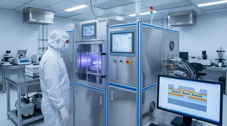
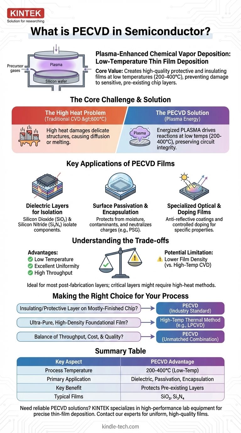
In semiconductor manufacturing, Plasma-Enhanced Chemical Vapor Deposition (PECVD) is a critical process used to deposit thin, uniform films of material onto a silicon wafer at low temperatures. It uses an energized plasma to drive the chemical reactions, which avoids the high heat required by traditional methods that could otherwise damage the sensitive, pre-existing layers of a microchip.
The central value of PECVD is its ability to create high-quality protective and insulating films without the destructive high temperatures of other deposition processes. This low-temperature capability is what makes the fabrication of complex, multi-layered integrated circuits possible.
The Core Challenge: Adding Layers Without Destroying the Chip
In semiconductor fabrication, a chip is built vertically, layer by layer. After a complex pattern of transistors and wires is created, new films must be added on top for insulation, protection, or to form other structures.
The Problem with High Heat
Many traditional deposition methods, like standard Chemical Vapor Deposition (CVD), require extremely high temperatures (often >600°C) to work.
This level of heat is destructive. It can cause the delicate, microscopic structures already on the wafer to melt, diffuse into each other, or otherwise change their properties, ruining the entire device.
How PECVD Solves the Problem
PECVD introduces a third ingredient to the process: plasma. By applying an electric field to the precursor gases, they are ionized into a state of matter known as plasma.
The energy for the chemical reaction now comes from this energized plasma, not from intense heat. This allows the deposition to occur at much lower temperatures (typically 200-400°C), preserving the integrity of the underlying circuits.
Key Applications of PECVD Films
Because it is both effective and non-destructive, PECVD is a workhorse process used to create several essential types of films on a wafer.
Dielectric Layers for Isolation
The most common use of PECVD is to deposit dielectric (electrically insulating) films like silicon dioxide (SiO₂) and silicon nitride (Si₃N₄).
These films are deposited between metal layers to prevent electrical shorts, effectively isolating the billions of individual components and connections within a modern processor.
Surface Passivation and Encapsulation
PECVD films serve as a protective barrier. They passivate the surface of the chip, neutralizing stray electrical charges, and encapsulate the device to shield it from moisture, mobile ions, and other contaminants that could cause it to fail.
A common example is the deposition of phosphosilicate glass (PSG), which provides excellent protective properties.
Specialized Optical and Doping Films
The process is also versatile enough to create films with specific optical properties, such as anti-reflective coatings used in CMOS image sensors and solar cells.
Furthermore, it can be used to deposit doped films, which serve as a source for introducing impurity atoms that alter the electrical properties of the silicon in a controlled way.
Understanding the Trade-offs
While indispensable, PECVD is not the only deposition method, and choosing it involves specific trade-offs.
The Clear Advantage: Low Temperature
The ability to process at low temperatures is PECVD's defining benefit. It is the default choice for any deposition step that occurs after temperature-sensitive devices have already been fabricated on the wafer.
The Production Advantage: Uniformity and Throughput
Modern PECVD systems provide excellent film uniformity across the entire surface of a large wafer, which is critical for achieving high manufacturing yields.
The process is also relatively fast, enabling high throughput that makes it economically viable for mass production.
The Potential Limitation: Film Density
Because PECVD is a lower-energy process than high-temperature thermal CVD, the resulting films can sometimes be less dense and contain more hydrogen impurities.
For many applications like isolation and encapsulation, this is perfectly acceptable. However, for the most critical, foundational layers of a transistor (like the gate oxide), a higher-temperature, higher-purity method may be required.
Making the Right Choice for Your Process
Your choice of deposition method is dictated entirely by the film's purpose and its position in the manufacturing sequence.
- If your primary focus is depositing an insulating or protective layer on a mostly-finished chip: PECVD is the industry-standard solution due to its low-temperature processing.
- If your primary focus is creating an ultra-pure, high-density foundational film early in the process: A high-temperature thermal method like LPCVD might be chosen, as no sensitive structures exist on the wafer yet.
- If your primary focus is balancing throughput, cost, and quality for mass production: PECVD offers an unmatched combination of speed and film performance for a wide range of applications.
Ultimately, PECVD is a cornerstone technology that enables the immense complexity and vertical integration of modern semiconductor devices.
Summary Table:
| Key Aspect | PECVD Advantage |
|---|---|
| Process Temperature | 200-400°C (Low-Temp) |
| Primary Application | Dielectric Layers, Passivation, Encapsulation |
| Key Benefit | Protects pre-existing chip layers from heat damage |
| Typical Films | Silicon Dioxide (SiO₂), Silicon Nitride (Si₃N₄) |
Need reliable PECVD solutions for your semiconductor fabrication? KINTEK specializes in high-performance lab equipment and consumables for precise thin-film deposition. Our expertise ensures uniform, high-quality films for your insulation and passivation layers, enhancing your chip yield and device reliability. Contact our experts today to discuss how our PECVD systems can meet your laboratory's specific semiconductor manufacturing needs!
Visual Guide
Related Products
- Inclined Rotary Plasma Enhanced Chemical Vapor Deposition PECVD Equipment Tube Furnace Machine
- Chemical Vapor Deposition CVD Equipment System Chamber Slide PECVD Tube Furnace with Liquid Gasifier PECVD Machine
- Inclined Rotary Plasma Enhanced Chemical Vapor Deposition PECVD Equipment Tube Furnace Machine
- RF PECVD System Radio Frequency Plasma-Enhanced Chemical Vapor Deposition RF PECVD
- Multi Heating Zones CVD Tube Furnace Machine Chemical Vapor Deposition Chamber System Equipment
People Also Ask
- How does PECVD facilitate Ru-C nanocomposite films? Precision Low-Temperature Thin Film Synthesis
- What is plasma enhanced chemical vapour deposition PECVD used for? Enable Low-Temp Thin Films for Electronics & Solar
- What is plasma enhanced chemical vapor deposition PECVD equipment? A Guide to Low-Temperature Thin Film Deposition
- What are the advantages of plasma enhanced chemical vapor deposition? Enable Low-Temperature, High-Quality Film Deposition
- How does plasma enhanced chemical vapor deposition work? Enable Low-Temperature Thin Film Deposition


