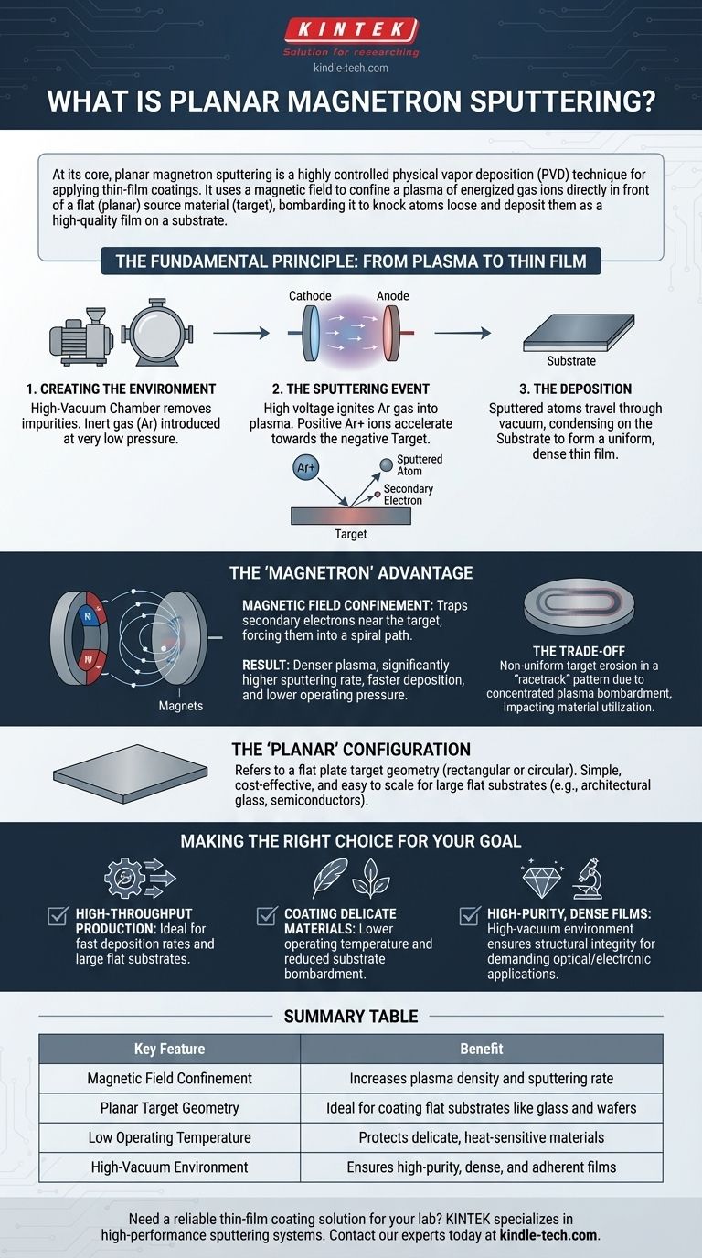
At its core, planar magnetron sputtering is a highly controlled physical vapor deposition (PVD) technique for applying thin-film coatings. It uses a magnetic field to confine a plasma of energized gas ions directly in front of a flat (planar) source material, called the target. These ions bombard the target, physically knocking atoms loose, which then travel through a vacuum and deposit onto a substrate to form a uniform, high-quality film.
The essential innovation of magnetron sputtering is the strategic use of a magnetic field to trap electrons near the target. This creates a dense, highly efficient plasma that dramatically increases the coating speed and lowers the operating pressure, all while protecting the substrate from damaging heat and bombardment.
The Fundamental Principle: From Plasma to Thin Film
To understand magnetron sputtering, it's best to break the process down into its core stages. Each step builds upon the last in a precisely controlled vacuum environment.
Creating the Environment: Vacuum and Inert Gas
The entire process takes place within a high-vacuum chamber. This is critical for removing impurities that could contaminate the final film.
Once a vacuum is established, an inert gas, most commonly argon, is introduced at very low pressure. This gas provides the atoms that will be ionized to create the plasma.
The Sputtering Event: Ion Bombardment
A high negative voltage is applied to the target, which is the source material for the coating. This creates a strong electric field between the target (cathode) and the chamber/anode.
This voltage ignites the argon gas, stripping electrons from the atoms and creating a glowing plasma composed of positive argon ions and free electrons. The positive argon ions are then aggressively accelerated toward the negatively charged target.
Upon impact, these high-energy ions physically knock out, or "sputter," atoms from the target material.
The Deposition: Film Formation on the Substrate
The sputtered atoms are ejected from the target and travel through the vacuum chamber.
When these atoms reach the substrate (the object being coated), they condense on its surface, gradually building up a thin, dense, and highly adherent film.
The "Magnetron" Advantage: Why Magnets Are the Key
Standard sputtering works, but it is slow and inefficient. The addition of a magnetron—a specific arrangement of magnets behind the target—revolutionizes the process.
Trapping Electrons for Maximum Efficiency
When ions strike the target, they not only sputter atoms but also knock loose secondary electrons. In a simple system, these electrons would be lost.
A magnetron creates a magnetic field parallel to the target's surface. This field traps the energetic electrons, forcing them into a long, spiral path directly in front of the target.
The Result: Denser Plasma and Faster Deposition
As these trapped electrons spiral, they collide with and ionize a much larger number of neutral argon atoms than they otherwise would.
This action dramatically increases the density of the plasma in the most effective region—right by the target. More ions mean more bombardment, which results in a significantly higher sputtering rate and faster film deposition.
Understanding the Trade-offs
The primary trade-off in planar magnetron sputtering is non-uniform target erosion. The magnetic field confines the plasma most intensely in a specific area, often shaped like an oval or a "racetrack."
This concentrated bombardment causes the target to erode unevenly in this racetrack pattern. Over time, this requires target replacement even when significant material remains outside the erosion groove, impacting material utilization efficiency.
The "Planar" Configuration
The term "planar" simply refers to the geometry of the target material.
The Simplicity of a Flat Target
In this configuration, the target is a flat plate, typically rectangular or circular. This is the most common, cost-effective, and straightforward setup for coating flat substrates or large batches of smaller components.
Its simple geometry makes it easy to design, scale, and maintain, which is why it is ubiquitous in industrial applications for coating things like architectural glass, semiconductors, and displays.
Making the Right Choice for Your Goal
Planar magnetron sputtering is not a one-size-fits-all solution, but it is a powerful and versatile tool when applied to the right problem.
- If your primary focus is high-throughput production of uniform coatings: This method is ideal for its fast deposition rates and scalability for coating large, flat substrates.
- If your primary focus is coating delicate or temperature-sensitive materials: The process's lower operating temperature and reduced electron bombardment on the substrate make it a superior choice over other thermal methods.
- If your primary focus is achieving high-purity, dense films with strong adhesion: The high-vacuum environment and energetic deposition process create coatings with excellent structural integrity for demanding optical or electronic applications.
Ultimately, understanding this process empowers you to select the most efficient and precise method for creating advanced material surfaces.
Summary Table:
| Key Feature | Benefit |
|---|---|
| Magnetic Field Confinement | Increases plasma density and sputtering rate |
| Planar Target Geometry | Ideal for coating flat substrates like glass and wafers |
| Low Operating Temperature | Protects delicate, heat-sensitive materials |
| High-Vacuum Environment | Ensures high-purity, dense, and adherent films |
Need a reliable thin-film coating solution for your lab? KINTEK specializes in high-performance lab equipment, including sputtering systems designed for precision and efficiency. Whether you're working in semiconductor research, optics, or materials science, our planar magnetron sputtering tools deliver the uniform, high-quality coatings you need. Contact our experts today to discuss how we can support your specific laboratory requirements!
Visual Guide
Related Products
- Microwave Plasma Chemical Vapor Deposition MPCVD Machine System Reactor for Lab and Diamond Growth
- Inclined Rotary Plasma Enhanced Chemical Vapor Deposition PECVD Equipment Tube Furnace Machine
- Chemical Vapor Deposition CVD Equipment System Chamber Slide PECVD Tube Furnace with Liquid Gasifier PECVD Machine
- Inclined Rotary Plasma Enhanced Chemical Vapor Deposition PECVD Equipment Tube Furnace Machine
- High Energy Planetary Ball Mill Milling Machine for Laboratory
People Also Ask
- How does a microwave plasma reactor facilitate the synthesis of diamond? Master MPCVD with Precision Technology
- What is microwave plasma chemical vapor deposition? A Guide to High-Purity Diamond Film Growth
- What are the primary advantages of the CVD method for growing diamonds? Engineering High-Purity Gems and Components
- Why is argon-rich gas phase chemistry used for UNCD growth? Unlock Precision Nano-Diamond Synthesis
- How is a diamond formed from CVD? The Science of Growing Diamonds Atom by Atom