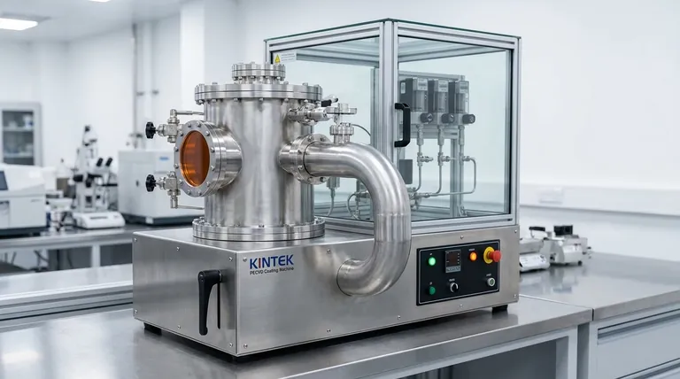
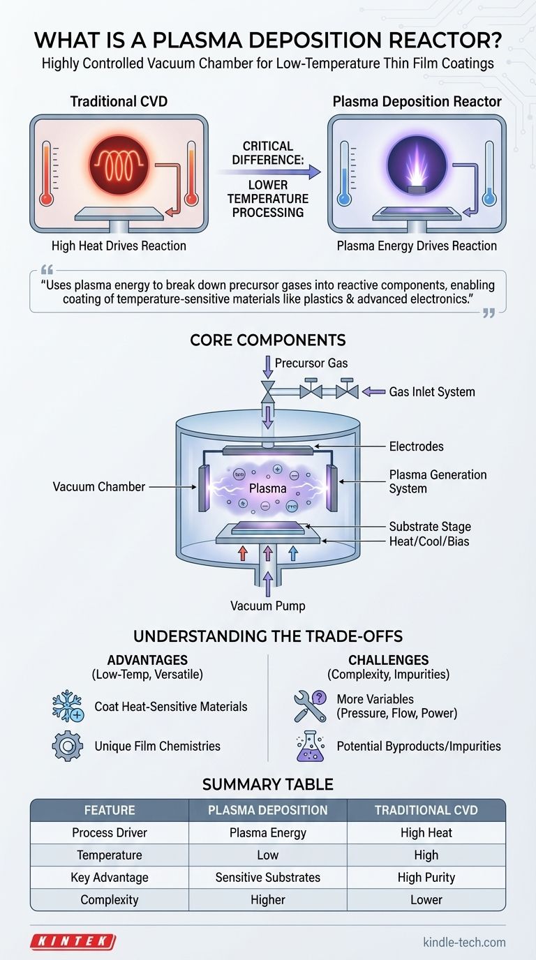
A plasma deposition reactor is a highly controlled vacuum chamber designed to grow thin, durable coatings onto a surface using an energized gas known as plasma. It is a specialized form of a chemical vapor deposition (CVD) system, but with a critical difference: instead of relying solely on high heat to trigger chemical reactions, it uses plasma to activate the coating materials. This allows the deposition process to occur at significantly lower temperatures.
The central purpose of a plasma deposition reactor is to use the energy of plasma to break down precursor gases into reactive components. This fundamental shift from high heat to plasma energy makes it possible to coat temperature-sensitive materials, such as plastics and advanced electronics, with high-performance thin films.
Deconstructing the Plasma Deposition Process
To understand the reactor, you must first understand the process it enables. It is a powerful evolution of a well-established industrial technique.
The Foundation: Chemical Vapor Deposition (CVD)
In traditional CVD, a part (or "substrate") is placed inside a reaction chamber.
A specific gas or vapor containing the coating material is introduced. High temperatures cause this gas to react and decompose, leaving a solid layer of the desired material on the part's surface.
The Enhancement: Introducing Plasma
A plasma deposition reactor adds another step: it generates plasma.
Plasma is often called the fourth state of matter. It is a gas that has been energized—typically by a strong electric field—until its atoms are broken apart into a soup of charged ions, electrons, and highly reactive neutral species called radicals.
How Plasma Changes the Game
The immense energy contained within the plasma provides the activation energy needed for the chemical reactions.
The highly reactive radicals created in the plasma readily bond to the substrate surface, building the coating layer by layer.
Because the plasma, not heat, drives the reaction, the entire process can run at much lower temperatures. This is the single most important advantage of the technology.
Core Components of a Plasma Deposition Reactor
While designs vary, nearly all plasma deposition reactors share a common set of functional components.
The Vacuum Chamber
This is the sealed enclosure (the "kettle body") where the entire process takes place. It is pumped down to a near-vacuum to remove air and other contaminants that could interfere with the reaction.
The Gas Inlet System
A precision-controlled system of valves and mass flow controllers introduces one or more precursor gases into the chamber. The exact mixture and flow rate of these gases determine the final coating's chemical composition.
The Plasma Generation System
This is the heart of the reactor. It typically consists of electrodes connected to a power source (like a radio frequency or DC supply). When activated, it creates a powerful electric field that ignites the gas into a glowing plasma.
The Substrate Stage
This is where the object to be coated is placed. This stage can often be heated, cooled, or electrically biased to give engineers another layer of control over the film's final properties, such as its density and adhesion.
Understanding the Trade-offs
Using plasma provides powerful benefits, but it also introduces unique challenges that must be managed.
The Primary Advantage: Low-Temperature Processing
The ability to deposit hard, dense coatings on materials that cannot withstand high heat is revolutionary. This opens up applications for plastics, polymers, and complex electronic devices.
The Challenge: Process Complexity
A plasma process has more variables than a thermal one. Engineers must precisely control gas pressure, gas flow rates, RF power, frequency, and substrate temperature. A small deviation in any parameter can significantly alter the coating's characteristics.
The Limitation: Potential Impurities
The chemical reactions in plasma are complex and can create unintended byproducts. For example, if using a hydrocarbon gas, hydrogen atoms can become embedded in the final film, which can affect its hardness or optical properties. This requires careful process tuning to mitigate.
Making the Right Choice for Your Goal
The decision to use a plasma-based process hinges entirely on the properties of your substrate and the desired outcome of the coating.
- If your primary focus is coating heat-sensitive materials: Plasma-enhanced deposition is often the only viable choice, as it bypasses the need for destructive high-temperature reactions.
- If your primary focus is maximum film purity and density: Traditional high-temperature CVD may be superior for certain materials, as the extreme heat can help create a more perfect crystalline structure with fewer impurities.
- If your primary focus is versatility and novel materials: Plasma deposition excels by enabling the creation of unique film chemistries from gas combinations that would not react under thermal conditions alone.
Ultimately, the plasma reactor is a critical tool for modern materials science, enabling the creation of advanced coatings that would otherwise be impossible to produce.
Summary Table:
| Feature | Plasma Deposition Reactor | Traditional CVD |
|---|---|---|
| Process Driver | Plasma Energy | High Heat |
| Temperature | Low (Ideal for sensitive substrates) | High |
| Key Advantage | Coats plastics & electronics | High film purity |
| Complexity | Higher (more variables to control) | Lower |
Ready to enhance your materials with precision thin-film coatings? KINTEK specializes in advanced lab equipment, including plasma deposition reactors, to help you coat temperature-sensitive substrates like plastics and electronics with high-performance films. Our expertise ensures you get the right solution for your specific research or production needs. Contact our experts today to discuss how we can support your laboratory's coating challenges!
Visual Guide
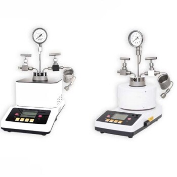
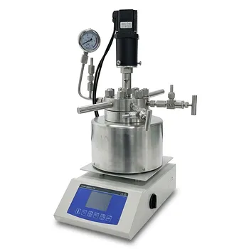
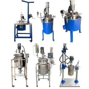
Related Products
- Microwave Plasma Chemical Vapor Deposition MPCVD Machine System Reactor for Lab and Diamond Growth
- 915MHz MPCVD Diamond Machine Microwave Plasma Chemical Vapor Deposition System Reactor
- Cylindrical Resonator MPCVD Machine System Reactor for Microwave Plasma Chemical Vapor Deposition and Lab Diamond Growth
- Chemical Vapor Deposition CVD Equipment System Chamber Slide PECVD Tube Furnace with Liquid Gasifier PECVD Machine
- RF PECVD System Radio Frequency Plasma-Enhanced Chemical Vapor Deposition RF PECVD
People Also Ask
- What are the primary advantages of the CVD method for growing diamonds? Engineering High-Purity Gems and Components
- What pressure is needed for chemical vapor deposition of diamonds? Master the Low-Pressure 'Sweet Spot'
- What is microwave plasma chemical vapor deposition? A Guide to High-Purity Diamond Film Growth
- What are the advantages of a Microwave Plasma CVD reactor for MCD/NCD coatings? Precision Multilayer Diamond Engineering
- How do vacuum pumps and valves collaborate in MPCVD? Achieve Precise Pressure Control for Superior CNT Synthesis