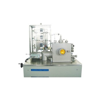
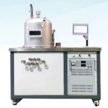
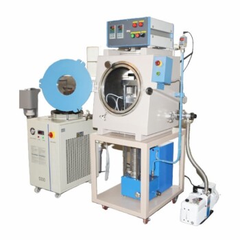
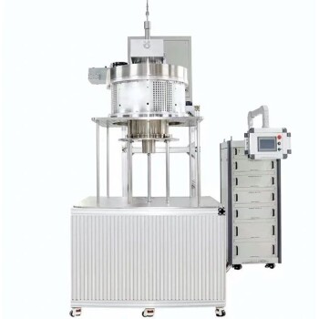
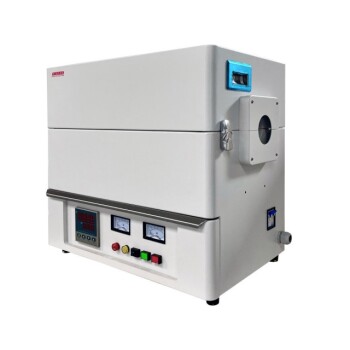
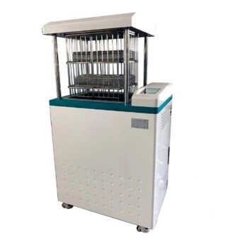
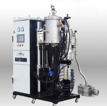
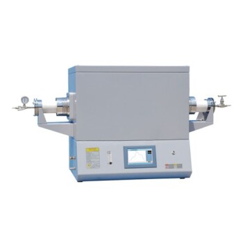
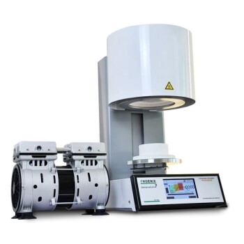
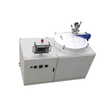
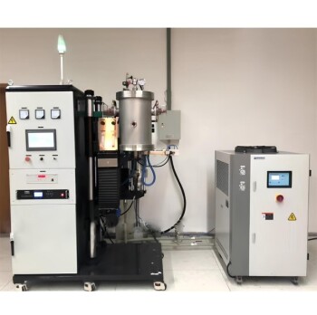
At its core, Plasma-Enhanced Chemical Vapor Deposition (PECVD) equipment is a sophisticated vacuum system used to deposit exceptionally thin, high-performance films onto a substrate. Unlike traditional Chemical Vapor Deposition (CVD) which relies on extreme heat to trigger chemical reactions, PECVD equipment uses an electrically charged gas—a plasma—to create reactive molecules. This fundamental difference allows the deposition process to occur at significantly lower temperatures.
The central purpose of PECVD equipment is to overcome the temperature limitations of conventional deposition methods. By using plasma as an energy source instead of pure heat, it enables the coating of temperature-sensitive materials and provides unique control over the final film's structural and mechanical properties.
How PECVD Equipment Works: From Gas to Solid Film
PECVD equipment integrates standard vacuum deposition components with a specialized system for generating and sustaining plasma. The process is a controlled, multi-step sequence inside a reaction chamber.
The Core Components
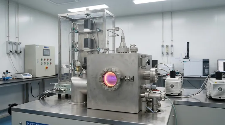
A typical PECVD system is built around several critical subsystems:
- Reaction Chamber: A vacuum-sealed chamber where the substrate is placed and the deposition occurs.
- Gas Delivery System: Precisely mixes and introduces precursor gases into the chamber.
- Vacuum System: Pumps that remove air and maintain the ultra-low pressures required for the process.
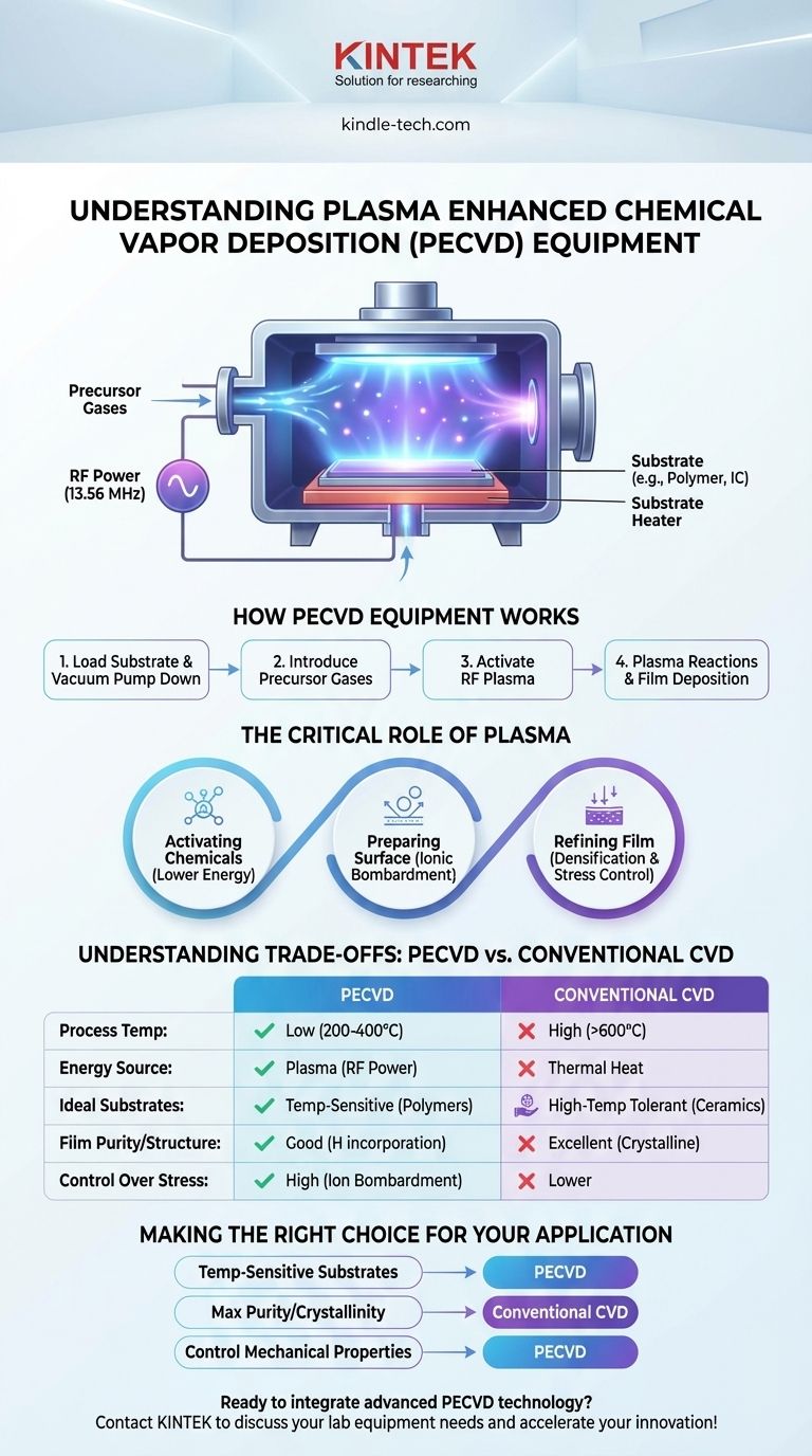
- Energy Source: An RF (Radio Frequency) power supply, often at 13.56 MHz, connected to electrodes inside the chamber to ignite and sustain the plasma.
- Substrate Heater: Provides low-level, controlled heat to the substrate to promote surface reactions.
- Control System: Automates and monitors all parameters, including gas flow, pressure, RF power, and temperature.
The Process Flow
The deposition process begins by placing a substrate inside the chamber and pumping the system down to a high vacuum. Precursor gases are then introduced at a controlled rate.
Next, the RF energy source is activated. This energy ionizes the gas, stripping electrons from atoms and creating a mixture of ions, electrons, and highly reactive neutral radicals. This glowing, energized state is the plasma.
These reactive radicals then diffuse and adsorb onto the substrate surface, where they react to form the desired solid film, layer by layer.
The Critical Role of Plasma
The plasma is not merely a heat substitute; it fundamentally changes the deposition environment and provides multiple advantages over thermally-driven processes.
Activating Chemicals Without Extreme Heat
The primary function of the plasma is to provide energy for dissociation. High-energy electrons in the plasma collide with stable precursor gas molecules, breaking them into the reactive species (radicals) needed for film growth.
This process happens at a fraction of the thermal energy required in conventional CVD, effectively acting as a chemical shortcut.
Preparing the Surface for Deposition
Ions from the plasma are accelerated towards the substrate, bombarding its surface with low energy. This ionic bombardment serves a critical purpose by creating dangling bonds—atomic-level "docking points" that significantly improve the adhesion of the depositing film.
Refining the Film in Real-Time
The ion bombardment also helps to densify the growing film by compacting the atomic structure. Furthermore, it can selectively etch away weakly bonded atoms or impurities from the surface.
This constant refinement during growth is how PECVD allows for precise control over the film's internal stress and density, which are critical for its mechanical and optical performance.
Understanding the Trade-offs: PECVD vs. Conventional CVD
Choosing between PECVD and conventional CVD depends entirely on the material requirements and the substrate's limitations. They are not interchangeable technologies.
The Temperature Advantage
This is PECVD's defining strength. Its low-temperature nature (typically 200-400°C) allows for the coating of substrates that would be damaged or destroyed by high-temperature CVD (often >600°C), such as polymers, plastics, and certain semiconductor devices.
Film Quality and Purity
Because conventional CVD relies on high thermal energy, it often produces films with higher purity and a more ordered, crystalline structure.
PECVD films, due to the complex plasma chemistry, can sometimes incorporate other elements (like hydrogen from precursor gases) into the film. While sometimes a desired feature, this can be considered an impurity in applications demanding the highest material purity.
Deposition Rate and Control
PECVD generally offers higher deposition rates than low-temperature CVD alternatives. The ability to independently control plasma power, gas flow, and temperature gives engineers more levers to pull to tune film properties like stress, refractive index, and hardness.
Making the Right Choice for Your Application
Selecting the correct deposition technology requires matching the process capabilities to your end goal.
- If your primary focus is coating temperature-sensitive substrates like polymers or integrated circuits: PECVD is the superior choice because its plasma-driven process avoids the damaging high heat of conventional methods.
- If your primary focus is achieving maximum film purity and crystallinity for demanding optical or electronic layers: Traditional high-temperature CVD may be necessary, provided your substrate can withstand the heat.
- If your primary focus is controlling mechanical properties like film stress and density: PECVD offers unique advantages through ion bombardment, which actively refines the film's structure as it grows.
Ultimately, understanding PECVD is understanding how to strategically use a different form of energy—plasma instead of just heat—to construct high-performance materials from the atom up.
Summary Table:
| Feature | PECVD | Conventional CVD |
|---|---|---|
| Process Temperature | Low (200-400°C) | High (>600°C) |
| Primary Energy Source | Plasma (RF Power) | Thermal Energy (Heat) |
| Ideal Substrates | Temperature-sensitive (polymers, ICs) | High-temperature tolerant (silicon, ceramics) |
| Film Purity/Crystallinity | Good (can incorporate elements like hydrogen) | Excellent (high purity, crystalline) |
| Control Over Film Stress/Density | High (via ion bombardment) | Lower |
Ready to integrate advanced PECVD technology into your lab?
KINTEK specializes in providing high-performance lab equipment and consumables, including state-of-the-art PECVD systems. Our solutions are designed to meet the precise demands of modern laboratories, enabling you to deposit high-quality thin films on even the most temperature-sensitive substrates.
We understand that choosing the right deposition technology is critical to your research and production success. Our experts are here to help you select the perfect PECVD equipment for your specific application, ensuring optimal performance and results.
Contact KINTEL today to discuss your PECVD needs and discover how our specialized lab equipment can accelerate your innovation!
Visual Guide
Related Products
- Inclined Rotary Plasma Enhanced Chemical Vapor Deposition PECVD Equipment Tube Furnace Machine
- RF PECVD System Radio Frequency Plasma-Enhanced Chemical Vapor Deposition RF PECVD
- HFCVD Machine System Equipment for Drawing Die Nano-Diamond Coating
- Vacuum Hot Press Furnace Machine for Lamination and Heating
- 915MHz MPCVD Diamond Machine Microwave Plasma Chemical Vapor Deposition System Reactor
People Also Ask
- Why does a PECVD vacuum system require both a rotary vane and turbo pump? Ensure High-Purity Coatings
- What is the process of PECVD in semiconductor? Enabling Low-Temperature Thin Film Deposition
- Can plasma enhanced CVD deposit metals? Why PECVD is rarely used for metal deposition
- Why is a Matching Network Indispensable in RF-PECVD for Siloxane Films? Ensure Stable Plasma and Uniform Deposition
- What are different types of thin films? A Guide to Function, Material, and Deposition Methods
