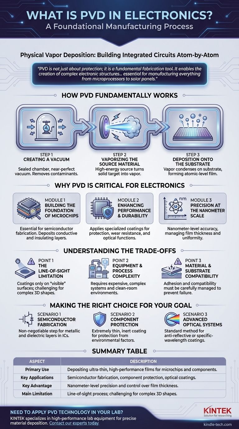
In electronics, PVD is a foundational manufacturing process. Physical Vapor Deposition (PVD) is a technique used in a high-vacuum environment to apply extremely thin, high-performance films of material onto a component, such as a silicon wafer or microchip. This process isn't merely a coating; it is how many of the essential conductive and insulating layers of modern integrated circuits are precisely constructed at an atomic level.
The critical takeaway is that PVD is not just about protection; it is a fundamental fabrication tool. It enables the creation of complex electronic structures by depositing specific materials atom-by-atom, which is essential for manufacturing everything from microprocessors to solar panels.
How PVD Fundamentally Works
The PVD process can be thought of as a highly controlled, atomic-level "spray-painting" that occurs inside a vacuum. It consists of three primary stages that are common across its various specific methods.
Step 1: Creating a Vacuum
First, the component to be coated (the substrate) and the material to be deposited (the target) are placed inside a sealed chamber. All the air is pumped out to create a near-perfect vacuum.
This vacuum is critical because it removes atmospheric particles that could otherwise contaminate the film or interfere with the deposition process.
Step 2: Vaporizing the Source Material
Next, a high-energy source is aimed at the target material. This energy, which can come from a plasma or an electron beam, is powerful enough to knock atoms loose from the solid target, turning it into a vapor.
These vaporized atoms now travel freely through the vacuum chamber.
Step 3: Deposition onto the Substrate
The vaporized atoms travel in a straight line until they strike the cooler substrate. Upon impact, they condense and form a very thin, uniform, and tightly bonded film on the surface of the electronic component.
This deposition is controlled with extreme precision, often building layers that are only a few atoms thick.
Why PVD is Critical for Electronics
While PVD is used in many industries, it is indispensable in electronics manufacturing due to its precision and the unique properties of the films it creates.
Building the Foundation of Microchips
The most important application of PVD in electronics is in semiconductor fabrication. It is used to deposit the ultra-thin layers of conductive metals (like aluminum or copper) and insulating materials that form the intricate circuits on a microchip.
Without PVD, the nanoscale structures of modern CPUs and memory chips would be impossible to build.
Enhancing Performance and Durability
PVD is also used to apply specialized coatings that improve a component's function. This includes durable protective films that shield sensitive parts from wear and corrosion or optical coatings on sensors and displays that reduce glare.
Precision at the Nanometer Scale
The primary advantage of PVD is its control. The process allows engineers to manage film thickness, composition, and uniformity with nanometer-level accuracy, ensuring the reliability and performance of microscopic electronic pathways.
Understanding the Trade-offs
Despite its advantages, PVD is not a universal solution. Understanding its limitations is key to appreciating its specific role in manufacturing.
The Line-of-Sight Limitation
PVD is a line-of-sight process. The vaporized atoms travel in straight lines, meaning they can only coat surfaces that are directly "visible" from the source material.
This makes it difficult to achieve a uniform coating on components with complex, three-dimensional shapes or deep trenches, which is a significant challenge in advanced chip design.
Equipment and Process Complexity
PVD systems are highly complex and expensive pieces of machinery that require carefully controlled clean-room environments. The process itself can be slow and energy-intensive, making it best suited for high-value, mass-produced components.
Material and Substrate Compatibility
The success of the PVD process depends on the properties of both the target material being deposited and the substrate receiving the coating. Adhesion, thermal expansion, and chemical compatibility must all be carefully managed to prevent film failure.
Making the Right Choice for Your Goal
The decision to use PVD is dictated by the precise engineering requirements of the electronic component.
- If your primary focus is semiconductor fabrication: PVD is a non-negotiable, essential step for depositing the metallic and dielectric layers that form transistors and interconnects on an integrated circuit.
- If your primary focus is component protection: PVD provides an extremely thin, hard, and inert coating that can protect sensitive electronics from environmental factors without adding significant size or weight.
- If your primary focus is advanced optical systems: PVD is the standard method for applying anti-reflective or specific-wavelength filtering coatings onto camera sensors, solar cells, and display panels.
Ultimately, Physical Vapor Deposition is one of the key enabling technologies that translates the design of a microchip into a physical reality.
Summary Table:
| Aspect | Description |
|---|---|
| Primary Use | Depositing ultra-thin, high-performance films for microchips and components. |
| Key Applications | Semiconductor fabrication, component protection, optical coatings for sensors and displays. |
| Key Advantage | Nanometer-level precision and control over film thickness and uniformity. |
| Main Limitation | Line-of-sight process; challenging for complex 3D shapes. |
Need to apply PVD technology in your lab? KINTEK specializes in high-performance lab equipment and consumables for precise material deposition. Our expertise can help you achieve the nanometer-scale accuracy required for semiconductor research and advanced electronics manufacturing. Contact our experts today to discuss how our solutions can enhance your fabrication processes.
Visual Guide
Related Products
- RF PECVD System Radio Frequency Plasma-Enhanced Chemical Vapor Deposition RF PECVD
- Split Chamber CVD Tube Furnace with Vacuum Station Chemical Vapor Deposition System Equipment Machine
- Chemical Vapor Deposition CVD Equipment System Chamber Slide PECVD Tube Furnace with Liquid Gasifier PECVD Machine
- VHP Sterilization Equipment Hydrogen Peroxide H2O2 Space Sterilizer
- 30T 40T Split Automatic Heated Hydraulic Press Machine with Heated Plates for Laboratory Hot Press
People Also Ask
- What are the benefits of PECVD? Achieve Superior Low-Temperature Thin Film Deposition
- Why does PECVD commonly use RF power input? For Precise Low-Temperature Thin Film Deposition
- How does RF power create plasma? Achieve Stable, High-Density Plasma for Your Applications
- What are the applications of PECVD? Essential for Semiconductors, MEMS, and Solar Cells
- What is plasma activated chemical vapour deposition method? A Low-Temperature Solution for Advanced Coatings