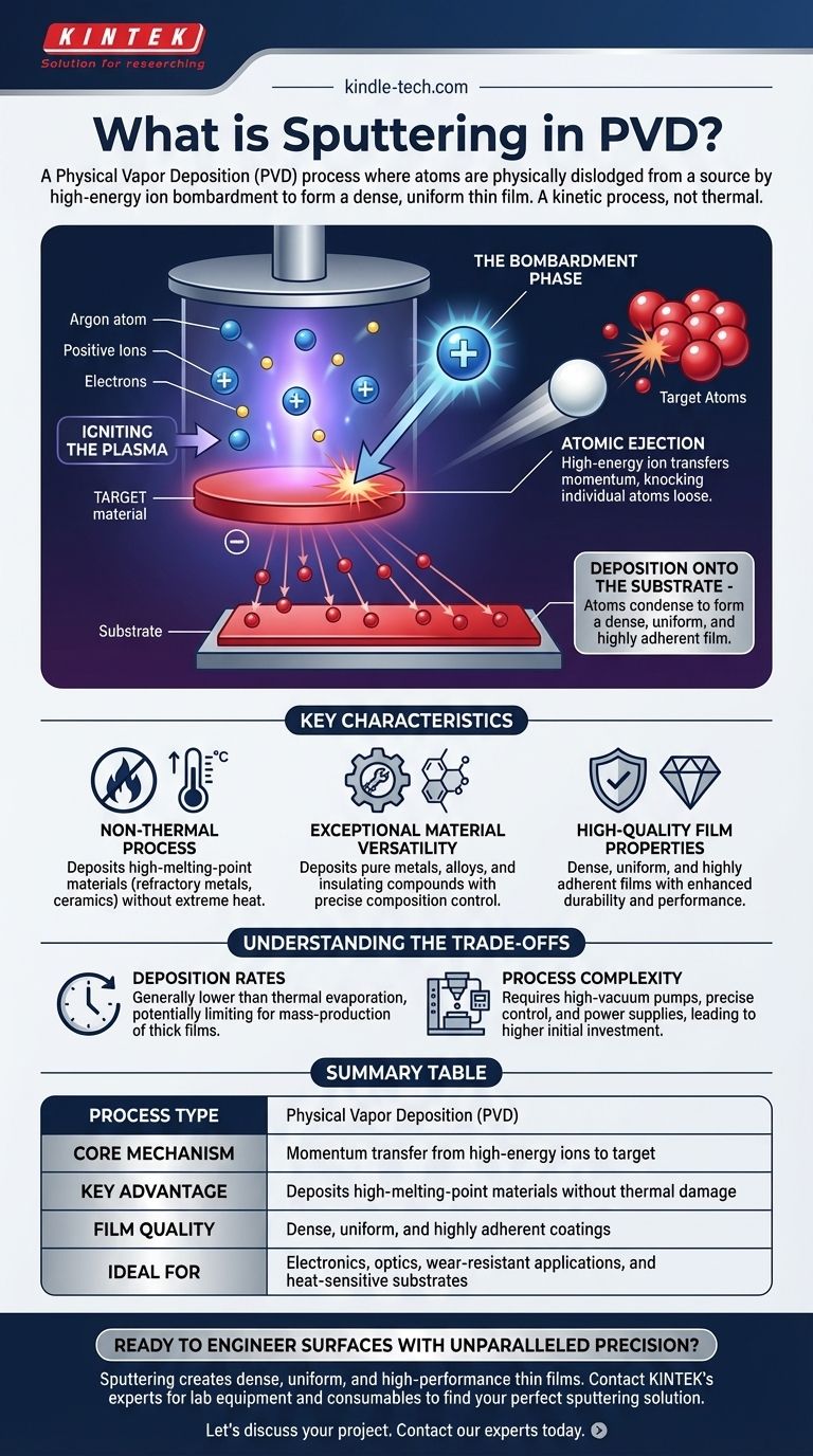
At its core, sputtering is a Physical Vapor Deposition (PVD) process where atoms are physically dislodged from a source material by high-energy ion bombardment. These ejected atoms then travel through a vacuum and condense onto a substrate, forming a dense and highly uniform thin film. It is a kinetic process, relying on momentum transfer rather than heat to vaporize the coating material.
Sputtering should be understood not as a melting or evaporation process, but as a microscopic game of billiards. High-energy ions act as the cue ball, striking a target material and knocking loose individual atoms, which then coat a nearby object.

The Core Mechanism: A Step-by-Step Breakdown
To understand sputtering, it is best to visualize it as a sequence of events occurring within a vacuum chamber. Each step is precisely controlled to achieve the desired film properties.
Igniting the Plasma
The process begins by introducing a small amount of an inert gas, almost always argon, into a high-vacuum chamber. A strong electric field is then applied, which strips electrons from the argon atoms. This creates plasma, a highly ionized state of matter consisting of positive argon ions and free electrons.
The Bombardment Phase
The material to be deposited, known as the target, is given a strong negative electrical charge. This negative potential powerfully attracts the positively charged argon ions from the plasma. These ions accelerate across the chamber and collide with the target surface with significant force.
Atomic Ejection
The collision is a purely physical event. The high-energy argon ion transfers its momentum to the atoms of the target material, much like a fast-moving billiard ball hitting a rack. This impact provides enough energy to knock individual atoms loose from the target's surface, ejecting them into the vacuum chamber.
Deposition onto the Substrate
These ejected, or "sputtered," atoms travel in a straight line until they strike a surface. The object to be coated, known as the substrate, is strategically placed to intercept these atoms. Upon arrival, the atoms condense on the substrate's surface, gradually building up a thin, dense, and highly adherent film.
Key Characteristics of the Sputtering Process
Sputtering is one of the most widely used PVD techniques because its unique characteristics offer significant advantages for a variety of applications.
A Non-Thermal Process
Unlike thermal evaporation, which melts material to create vapor, sputtering is a non-thermal vaporization process. This allows for the deposition of materials with extremely high melting points, such as refractory metals and ceramics, without needing to heat them to extreme temperatures.
Exceptional Material Versatility
Sputtering can deposit a vast range of materials, including pure metals, alloys, and even insulating compounds. Because the process transfers the target material's composition directly to the substrate, it is excellent for creating films from complex alloys with precise control.
High-Quality Film Properties
The sputtered atoms arrive at the substrate with higher kinetic energy compared to thermal evaporation. This energy helps create films that are incredibly dense, uniform, and well-adhered to the substrate surface. This results in durable and high-performance coatings.
Understanding the Trade-offs
While powerful, sputtering is not the universal solution for every PVD application. Understanding its limitations is crucial for making an informed decision.
Deposition Rates
Generally, sputtering can have a lower deposition rate compared to high-rate thermal evaporation processes. For applications requiring very thick films on a mass-production scale, this can be a limiting factor.
Process Complexity
The equipment required for sputtering—including high-vacuum pumps, multiple power supplies, and precise gas flow control—is more complex than that for simpler deposition methods. This can translate to higher initial capital investment.
Common Sputtering Variations
To overcome limitations and optimize performance, several specialized sputtering techniques exist. Methods like magnetron sputtering use magnetic fields to increase plasma density and deposition rates, while reactive sputtering introduces a reactive gas to form compound films like nitrides or oxides directly on the substrate.
Making the Right Choice for Your Goal
Selecting sputtering depends entirely on the required film characteristics and the material being deposited.
- If your primary focus is material versatility: Sputtering is the superior choice for depositing high-melting-point materials, complex alloys, or compounds that are difficult to evaporate.
- If your primary focus is film quality and adhesion: The energetic nature of sputtering produces dense, strongly bonded films ideal for demanding optical, electronic, or wear-resistant applications.
- If your primary focus is coating heat-sensitive substrates: Because it is a non-thermal process, sputtering can deposit high-performance films onto plastics or other materials that cannot withstand high temperatures.
Understanding sputtering as a controlled atomic transfer process unlocks its potential to engineer surfaces with unparalleled precision and performance.
Summary Table:
| Aspect | Description |
|---|---|
| Process Type | Physical Vapor Deposition (PVD) |
| Core Mechanism | Momentum transfer from high-energy ions (e.g., Argon) to a target material |
| Key Advantage | Deposits high-melting-point materials (metals, alloys, ceramics) without thermal damage |
| Film Quality | Dense, uniform, and highly adherent coatings |
| Ideal For | Electronics, optics, wear-resistant applications, and heat-sensitive substrates |
Ready to engineer surfaces with unparalleled precision?
Sputtering is the key to creating dense, uniform, and high-performance thin films for your most demanding applications. Whether you're working with complex alloys, high-melting-point ceramics, or heat-sensitive substrates, KINTEK's expertise in lab equipment and consumables can help you achieve superior results.
Let's discuss your project. Contact our experts today to find the perfect sputtering solution for your laboratory needs.
Visual Guide
Related Products
- RF PECVD System Radio Frequency Plasma-Enhanced Chemical Vapor Deposition RF PECVD
- Inclined Rotary Plasma Enhanced Chemical Vapor Deposition PECVD Equipment Tube Furnace Machine
- Chemical Vapor Deposition CVD Equipment System Chamber Slide PECVD Tube Furnace with Liquid Gasifier PECVD Machine
- Evaporation Boat for Organic Matter
- Electron Beam Evaporation Coating Oxygen-Free Copper Crucible and Evaporation Boat
People Also Ask
- What is the principle of plasma enhanced chemical vapor deposition? Achieve Low-Temperature Thin Film Deposition
- How are PECVD and CVD different? A Guide to Choosing the Right Thin-Film Deposition Process
- How does RF power create plasma? Achieve Stable, High-Density Plasma for Your Applications
- What are the applications of PECVD? Essential for Semiconductors, MEMS, and Solar Cells
- Why does PECVD commonly use RF power input? For Precise Low-Temperature Thin Film Deposition