In essence, sputtering is a process that deposits an ultra-thin layer of material onto a surface. It functions like an atomic-scale sandblaster, where high-energy ions bombard a source material (the "target"), knocking off individual atoms that then travel and coat a secondary surface (the "substrate") with a highly uniform and adherent film. This Physical Vapor Deposition (PVD) technique is fundamental to manufacturing countless modern devices, from semiconductor chips to optical lenses.
Sputtering's core value lies in its precision and control. By using energized ions to eject material atom-by-atom, it builds films with exceptional uniformity and adhesion that are difficult to achieve with other methods.
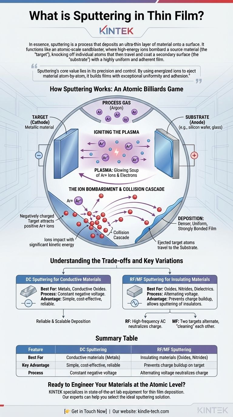
How Sputtering Works: An Atomic Billiards Game
Sputtering takes place within a vacuum chamber to ensure the purity of the film. The process can be visualized as a controlled chain reaction at the atomic level.
The Key Components
The chamber contains three critical elements: a target made of the material you want to deposit, a substrate which is the object you want to coat (like a silicon wafer or glass), and a small amount of an inert process gas, typically Argon.
Igniting the Plasma
A strong electric field is applied within the chamber, which strips electrons from the Argon gas atoms. This creates an energized state of matter known as plasma, a glowing soup of positive Argon ions and free electrons.
The Ion Bombardment
The negatively charged target (also called the cathode) powerfully attracts the positive Argon ions from the plasma. These ions accelerate and collide with the target's surface with significant kinetic energy.
The Collision Cascade
Each ion impact is like a subatomic cue ball striking a rack of billiard balls. The impact transfers momentum through the target's atomic lattice in a collision cascade. This chain reaction ejects atoms from the target's surface into the vacuum chamber.
Deposition onto the Substrate
These ejected target atoms travel through the low-pressure chamber and land on the substrate. Because they arrive with more energy than atoms from simple evaporation, they form a denser, more uniform, and more strongly bonded thin film across the entire surface.
Understanding the Trade-offs and Key Variations
While the principle is simple, the type of material being deposited dictates the specific sputtering technique required. The primary challenge revolves around electrical conductivity.
DC Sputtering for Conductive Materials
Direct Current (DC) sputtering is the most basic and common form. It uses a constant negative voltage on the target, making it ideal for depositing electrically conductive materials like metals and transparent conductive oxides. It is highly reliable and scalable.
The Challenge of Insulating Materials
If you use DC sputtering on an insulating (dielectric) target like silicon dioxide, the positive ions that strike it will accumulate on the surface. This buildup of positive charge, known as "target poisoning," eventually repels incoming ions and halts the sputtering process entirely.
RF and MF Sputtering for Non-Conductors
To deposit insulating materials, the charge buildup must be neutralized. This is achieved by rapidly alternating the voltage on the target.
- RF (Radio Frequency) Sputtering uses a high-frequency AC signal to alternate the voltage, allowing it to sputter any type of material.
- MF (Mid-Frequency AC) Sputtering often uses two targets that alternate as the cathode and anode, with each cycle effectively "cleaning" the other of charge buildup, ensuring a stable deposition process for non-conductive films.
Making the Right Choice for Your Goal
The decision of which sputtering method to use is almost always determined by the material you need to deposit.
- If your primary focus is depositing conductive materials (like metals): DC sputtering is the most straightforward, cost-effective, and reliable choice for your application.
- If your primary focus is depositing insulating or dielectric materials (like oxides or nitrides): You must use a technique like RF or MF sputtering to prevent charge buildup and ensure a stable process.
- If your primary focus is achieving the highest possible film quality and density: Sputtering is an excellent choice, as the higher energy of deposited atoms creates superior film adhesion and uniformity compared to many other techniques.
Mastering sputtering allows you to engineer material properties at the atomic level, making it an indispensable tool in modern technology.
Summary Table:
| Feature | DC Sputtering | RF/MF Sputtering |
|---|---|---|
| Best For | Conductive materials (Metals) | Insulating materials (Oxides, Nitrides) |
| Key Advantage | Simple, cost-effective, reliable | Prevents charge buildup on target |
| Process | Constant negative voltage | Alternating voltage neutralizes charge |
Ready to Engineer Your Materials at the Atomic Level?
Sputtering is essential for creating high-performance thin films with superior adhesion and uniformity. Whether you are developing semiconductor chips, optical coatings, or advanced sensors, choosing the right sputtering technique is critical to your success.
KINTEK specializes in providing state-of-the-art lab equipment and consumables for all your thin film deposition needs. Our experts can help you select the ideal sputtering solution—from DC for conductive metals to RF/MF for insulating oxides—ensuring precision and reliability for your specific application.
Contact us today to discuss how our sputtering solutions can enhance your research and production processes. Let's build the future, one atom at a time.
Visual Guide
Related Products
- Three-dimensional electromagnetic sieving instrument
- Chemical Vapor Deposition CVD Equipment System Chamber Slide PECVD Tube Furnace with Liquid Gasifier PECVD Machine
- Customer Made Versatile CVD Tube Furnace Chemical Vapor Deposition Chamber System Equipment
- Twin Screw Extruder Plastic Granulation Machine
- HFCVD Machine System Equipment for Drawing Die Nano-Diamond Coating
People Also Ask
- What is the advantage of sieving? A Simple, Reliable Method for Particle Size Analysis
- How is sieving important? The Critical Role of Particle Size Analysis in Quality Control
- Why is sieving equipment essential for the classification of processed bio-activated carbon? Optimize Performance
- Why is sieving equipment necessary for processing powder prior to hot extrusion of PEO? Ensure Cathode Film Uniformity
- What are the limitations of sieving? Understanding the Constraints of Particle Size Analysis