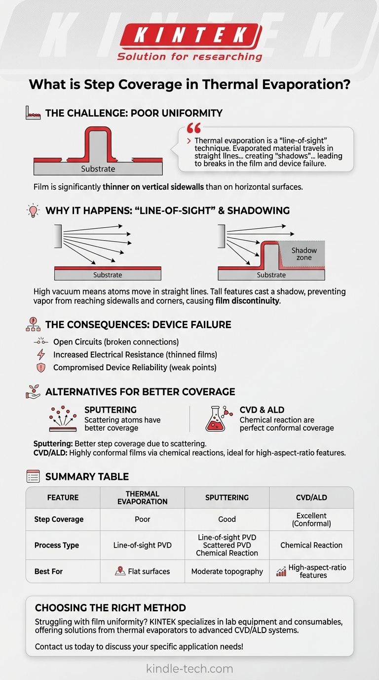
In thermal evaporation, step coverage describes how uniformly a deposited thin film covers the topography of a substrate, such as trenches or ridges. It is a critical measure of film continuity over three-dimensional features. Due to the nature of the process, thermal evaporation typically produces poor step coverage, resulting in films that are significantly thinner on vertical sidewalls than on horizontal surfaces.
The core issue is that thermal evaporation is a "line-of-sight" deposition technique. Evaporated material travels in straight lines from the source, creating "shadows" behind tall features on the substrate, which can lead to breaks in the film and device failure.
Why Thermal Evaporation Struggles with Step Coverage
Understanding why step coverage is a challenge comes down to the fundamental physics of the process. This limitation is not a flaw but an inherent characteristic of how the film is formed.
The "Line-of-Sight" Principle
Thermal evaporation occurs in a high vacuum, meaning atoms from the heated source material travel with very few collisions. They move in straight lines until they strike a surface.
Only the surfaces with a direct, unobstructed view of the evaporation source will be coated effectively.
The Shadowing Effect Explained
When a substrate has topography, like the edge of a patterned layer, this creates a "step." The top corner of this step blocks the incoming vapor from reaching the bottom corner and lower part of the sidewall.
This phenomenon is called shadowing. It's analogous to how a tall building casts a shadow, preventing sunlight from reaching the ground directly next to it.
The Consequence: Film Discontinuity
Because of shadowing, the film deposits thickly on the top horizontal surface but becomes progressively thinner down the vertical sidewall. At the bottom corner of the step, the film can be extremely thin or entirely absent.
This non-uniformity creates a weak point where the film is likely to be discontinuous, especially for taller steps or thicker films.
The Practical Impact of Poor Step Coverage
For many applications in microfabrication and electronics, poor step coverage is not just a geometric imperfection—it is a direct cause of device failure.
Open Circuits and Device Failure
The most severe consequence is a complete break in a conductive film, such as a metal interconnect. If a wire must run over a step, poor coverage can create an open circuit, preventing the device from functioning at all.
Increased Electrical Resistance
Even if the film is not completely broken, the thinned section at the step will have a significantly higher electrical resistance than the rest of the film. This can degrade device performance, generate excess heat, and create a point of failure.
Compromised Device Reliability
These thinned areas are mechanically and electrically weak. They are more susceptible to failure over time due to stresses like temperature cycling or electromigration, severely impacting the long-term reliability of the device.
Alternatives for Superior Coverage
When good step coverage is non-negotiable, thermal evaporation is often the wrong tool for the job. Other deposition techniques are specifically designed to create more uniform, or conformal, films.
Sputtering: A Step Up
Sputtering is another physical vapor deposition (PVD) method, but it operates at higher pressures than thermal evaporation. The deposited atoms scatter more, arriving at the substrate from a wider range of angles.
This reduces the shadowing effect and results in significantly better step coverage than thermal evaporation, though it is still not perfectly conformal.
CVD and ALD: The Gold Standard
Chemical Vapor Deposition (CVD) and Atomic Layer Deposition (ALD) are fundamentally different. They rely on chemical reactions on the substrate surface rather than a line-of-sight physical process.
Because the precursor gases can reach all exposed surfaces, these methods produce highly conformal films. ALD, in particular, offers near-perfect step coverage, making it the ideal choice for coating deep trenches and other high-aspect-ratio features.
Making the Right Choice for Your Process
Selecting the correct deposition method requires matching the technique's capabilities to your specific structural goals.
- If your primary focus is simplicity and cost on a flat surface: Thermal evaporation is an excellent choice for its purity and straightforward operation when step coverage is not a concern.
- If your primary focus is reliable electrical contacts over moderate topography: Sputtering offers a much-improved process window and better step coverage, ensuring film continuity.
- If your primary focus is perfect, uniform coverage in challenging geometries: Chemical Vapor Deposition (CVD) or Atomic Layer Deposition (ALD) are necessary to achieve the conformal films required for advanced devices.
Ultimately, choosing the right deposition tool depends entirely on understanding the topographical demands of your device.
Summary Table:
| Feature | Thermal Evaporation | Sputtering | CVD/ALD |
|---|---|---|---|
| Step Coverage | Poor | Good | Excellent (Conformal) |
| Process Type | Line-of-sight PVD | Scattered PVD | Chemical Reaction |
| Best For | Flat surfaces, simple coatings | Moderate topography, reliable contacts | High-aspect-ratio features, perfect uniformity |
Struggling with film uniformity over complex substrate features? KINTEK specializes in lab equipment and consumables, offering solutions from thermal evaporators to advanced CVD/ALD systems. Our experts can help you select the ideal deposition method to ensure film continuity, prevent device failure, and enhance your lab's performance. Contact us today to discuss your specific application needs!
Visual Guide
Related Products
- Molybdenum Tungsten Tantalum Evaporation Boat for High Temperature Applications
- Aluminized Ceramic Evaporation Boat for Thin Film Deposition
- Evaporation Boat for Organic Matter
- Chemical Vapor Deposition CVD Equipment System Chamber Slide PECVD Tube Furnace with Liquid Gasifier PECVD Machine
- Customer Made Versatile CVD Tube Furnace Chemical Vapor Deposition Chamber System Equipment
People Also Ask
- How does a molybdenum evaporation source function in H2S for MoS2 synthesis? Master Reactive Film Deposition
- What are thermal evaporation sources? Key Types and How to Choose the Right One
- What is the source of evaporation for thin film? Choosing Between Thermal and E-Beam Methods
- What is the widely used boat made of in thermal evaporation? Choosing the Right Material for High-Purity Deposition
- How source material is evaporated during deposition? A Guide to Resistive vs. E-Beam Methods