At its core, Chemical Vapor Deposition (CVD) is a process used to create high-performance, solid thin films and coatings. It works by introducing reactive precursor gases into a chamber where they decompose and react on a heated surface (the substrate), building up the desired material one atomic layer at a time.
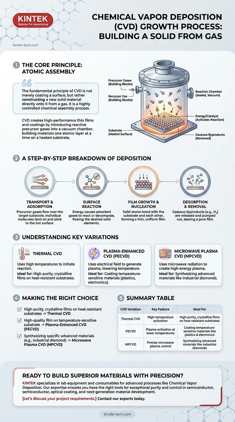
The fundamental principle of CVD is not merely coating a surface, but rather constructing a new solid material directly onto it from a gas. It is a highly controlled chemical assembly process that allows for the creation of materials with exceptional purity and specific properties that would be difficult to achieve otherwise.
The Core Principle: Building a Solid from Gas
To understand the CVD process, it's best to visualize it as a highly controlled and sterile environment where individual atoms are assembled into a structured layer.
The Environment: The Reaction Chamber
The entire process takes place inside a sealed reaction chamber. This chamber is typically held under a vacuum to remove any unwanted contaminants that could interfere with the chemical reaction and compromise the purity of the final film.
The Ingredients: Precursor Gases
The building blocks for the new material are introduced into the chamber as precursor gases. These are volatile chemical compounds that contain the elements required for the final film. For example, to create a silicon film, a precursor gas like silane (SiH₄) might be used.
The Catalyst: Activating the Reaction
Energy is required to break down the precursor gases and initiate the chemical reaction. Most commonly, this energy is high temperature, with the substrate being heated to hundreds or even thousands of degrees Celsius.
A Step-by-Step Breakdown of Deposition
While the specifics vary, the deposition process follows a clear sequence of events at the microscopic level.
Step 1: Transport and Adsorption
The precursor gases are transported into the chamber and flow over the target substrate. Individual gas molecules then land on and stick to the hot surface in a process called adsorption.
Step 2: Surface Reaction
Once adsorbed onto the hot surface, the energy from the substrate causes the precursor gases to decompose or react with other gases. This chemical reaction is the heart of the CVD process, where the desired solid elements are freed from the precursor gas.
Step 3: Film Growth and Nucleation
The solid atoms produced by the reaction begin to bond with the substrate and with each other. They diffuse across the surface to find stable growth sites, forming a thin, uniform film that builds up in thickness over time.
Step 4: Desorption and Removal
Gaseous byproducts from the reaction, such as hydrogen, are released from the surface (desorption) and are pumped out of the chamber, leaving only the pure, solid film behind.
Understanding the Key Variations
Not all CVD processes are the same. The method used to supply energy and activate the reaction is a critical distinction that defines the technique's applications and limitations.
Thermal CVD
This is the most fundamental form of CVD, relying solely on high temperatures to initiate the reaction. It is highly effective for creating extremely pure, crystalline films but is limited to substrates that can withstand the intense heat.
Plasma-Enhanced CVD (PECVD)
To deposit films on temperature-sensitive materials like plastics or certain electronics, PECVD is used. Instead of relying only on heat, this method uses an electrical field to generate a plasma within the chamber.
This high-energy plasma creates highly reactive molecular fragments at a much lower gas temperature, allowing the deposition to occur without damaging the underlying substrate. For example, in Microwave Plasma CVD (MPCVD), microwave radiation creates a plasma where electron temperatures can exceed 5000 K while the gas itself remains closer to 1000 K.
Why This Matters: Purity and Application
The precise control offered by CVD enables the creation of materials for highly demanding fields. It is essential in manufacturing semiconductors, optical coatings, and advanced materials like synthetic diamonds for industrial and electronic use. Its ability to produce cost-effective, high-purity materials makes it a cornerstone of modern technology.
Making the Right Choice for Your Goal
The specific CVD technique you choose depends entirely on the desired material properties and the limitations of your substrate.
- If your primary focus is creating high-purity, crystalline films and your substrate can handle high temperatures: Traditional thermal CVD offers unmatched quality and control.
- If your primary focus is depositing a high-quality film on a temperature-sensitive substrate: Plasma-Enhanced CVD (PECVD) is the ideal choice, as it uses plasma energy to reduce the required process temperature.
- If your primary focus is synthesizing a specific advanced material like industrial diamond: Specialized techniques like Microwave Plasma-assisted CVD (MPCVD) provide the precise conditions needed for exceptional properties.
Ultimately, mastering Chemical Vapor Deposition is about precisely controlling a chemical reaction to build superior materials from the atom up.
Summary Table:
| CVD Variation | Key Feature | Ideal For |
|---|---|---|
| Thermal CVD | High-temperature activation | High-purity, crystalline films on heat-resistant substrates |
| Plasma-Enhanced CVD (PECVD) | Plasma activation at lower temperatures | Coating temperature-sensitive materials like plastics and electronics |
| Microwave Plasma CVD (MPCVD) | Precise microwave plasma control | Synthesizing advanced materials like industrial diamonds |
Ready to build superior materials with precision?
KINTEK specializes in the lab equipment and consumables that power advanced processes like Chemical Vapor Deposition. Whether you are developing semiconductors, optical coatings, or next-generation materials, our expertise ensures you have the right tools for exceptional purity and control.
Let's discuss your project requirements. Contact our experts today to find the perfect CVD solution for your laboratory's needs.
Visual Guide
Related Products
- Chemical Vapor Deposition CVD Equipment System Chamber Slide PECVD Tube Furnace with Liquid Gasifier PECVD Machine
- HFCVD Machine System Equipment for Drawing Die Nano-Diamond Coating
- Customer Made Versatile CVD Tube Furnace Chemical Vapor Deposition Chamber System Equipment
- Split Chamber CVD Tube Furnace with Vacuum Station Chemical Vapor Deposition System Equipment Machine
- Inclined Rotary Plasma Enhanced Chemical Vapor Deposition PECVD Equipment Tube Furnace Machine
People Also Ask
- What happens during deposition chemistry? Building Thin Films from Gaseous Precursors
- What types of substrates are used in CVD to facilitate graphene films? Optimize Graphene Growth with the Right Catalyst
- What are the processes of vapor phase deposition? Understand CVD vs. PVD for Superior Thin Films
- What is plasma enhanced chemical vapor deposition PECVD equipment? A Guide to Low-Temperature Thin Film Deposition
- Why is Chemical Vapor Deposition (CVD) equipment uniquely suited for constructing hierarchical superhydrophobic structures?


