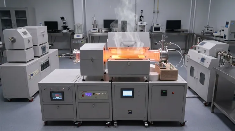
At its core, chemical vapor deposition (CVD) is a highly controlled process for building a solid, high-performance thin film on a surface from a chemical gas. It involves vaporizing one or more precursor materials, which then react and decompose on a heated substrate to "grow" the desired material layer by layer. This technique is fundamental to manufacturing advanced electronics, protective coatings, and novel materials.
Chemical vapor deposition is not a coating method in the traditional sense of spraying; it is a synthesis process. It uses controlled chemical reactions in a gas phase to construct a new solid material directly onto a substrate, enabling exceptional purity and structural control.
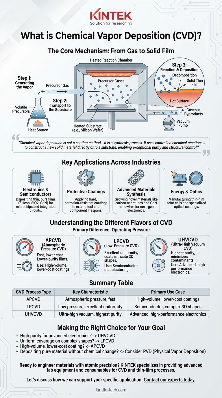
The Core Mechanism: From Gas to Solid Film
To understand CVD, it's best to think of it as a precise, multi-step assembly line at the molecular level. Each step is carefully controlled to achieve the final film's desired properties.
Step 1: Generating the Vapor
The process begins with volatile precursors, which are chemical compounds that contain the elements you want to deposit. These precursors are heated or have their pressure reduced to turn them into a gas.
This vapor is then precisely introduced into a reaction chamber.
Step 2: Transport to the Substrate
Once inside the chamber, the precursor gases flow towards the substrate. The substrate is the base material (like a silicon wafer, glass, or metal part) that will be coated.
Step 3: Reaction and Deposition
The substrate is heated to a specific temperature. When the precursor gases get near or make contact with this hot surface, they undergo a chemical reaction and decompose.
The desired solid elements bond to the substrate, forming a thin, uniform film. Other gaseous byproducts from the reaction are simply pumped out of the chamber.
Key Applications Across Industries
The precision of CVD makes it indispensable for creating materials and coatings that are impossible to produce otherwise.
Electronics and Semiconductors
This is the most common use of CVD. It is used to deposit incredibly thin, pure films of materials like silicon, silicon dioxide, and gallium nitride, which are the building blocks of microchips and integrated circuits.
Protective Coatings
CVD is used to apply extremely hard and corrosion-resistant coatings to cutting tools, engine components, and other industrial parts. These ceramic or metallic films dramatically extend the lifespan and performance of the underlying material.
Advanced Materials Synthesis
Researchers use CVD to "grow" novel materials with unique properties. This includes creating structures like carbon nanotubes and GaN nanowires, which have applications in next-generation electronics and composites.
Energy and Optics
In the manufacturing of thin-film solar cells, CVD is used to deposit the critical photovoltaic materials onto a substrate. It's also used for creating specialized optical coatings for lenses and sensors.
Understanding the Different Flavors of CVD
Not all CVD processes are the same. The primary difference between types of CVD is the operating pressure within the reaction chamber, which dictates the quality and characteristics of the final film.
The Importance of Pressure
Pressure controls how gas molecules move and interact. High pressure means more collisions and faster deposition, while low pressure allows for more uniform coverage on complex surfaces.
Atmospheric Pressure CVD (APCVD)
This is the simplest form, operating at normal atmospheric pressure. It's fast and relatively inexpensive but can result in lower-purity films.
Low-Pressure CVD (LPCVD)
By reducing the pressure, LPCVD allows the precursor gases to coat the substrate more evenly, even on intricate 3D shapes. This results in excellent film uniformity and is a workhorse process in the semiconductor industry.
Ultra-High Vacuum CVD (UHVCVD)
Operating at extremely low pressures, UHVCVD is used when the absolute highest purity is required. It minimizes the risk of contaminants and is crucial for creating advanced, high-performance semiconductor devices.
Making the Right Choice for Your Goal
The specific CVD method is chosen based on the desired outcome, balancing cost, speed, and the required quality of the final film.
- If your primary focus is high purity for advanced electronics: UHVCVD is the necessary choice to minimize defects and ensure peak performance.
- If your primary focus is uniform coverage over complex shapes: LPCVD provides an excellent balance of quality, conformity, and throughput.
- If your primary focus is high-volume, lower-cost coating: APCVD can be a viable option when absolute purity is not the primary concern.
- If your primary focus is depositing a pure material without a chemical change: You may need to consider a different technique, such as Physical Vapor Deposition (PVD), which uses physical means like evaporation to deposit films.
Ultimately, chemical vapor deposition is a versatile and powerful technique for engineering materials with precision from the atoms up.
Summary Table:
| CVD Process Type | Key Characteristic | Primary Use Case |
|---|---|---|
| APCVD | Atmospheric pressure, fast deposition | High-volume, lower-cost coatings |
| LPCVD | Low pressure, excellent uniformity | Semiconductor manufacturing, complex 3D shapes |
| UHVCVD | Ultra-high vacuum, highest purity | Advanced, high-performance electronics |
Ready to engineer materials with atomic precision?
KINTEK specializes in providing the advanced lab equipment and consumables necessary for chemical vapor deposition and other critical thin-film processes. Whether you are developing next-generation semiconductors, protective coatings, or novel materials like carbon nanotubes, our solutions support the high-purity, controlled environments essential for success.
Let's discuss how we can support your specific application: Contact our experts today to find the right tools for your research and production goals.
Visual Guide
Related Products
- Chemical Vapor Deposition CVD Equipment System Chamber Slide PECVD Tube Furnace with Liquid Gasifier PECVD Machine
- RF PECVD System Radio Frequency Plasma-Enhanced Chemical Vapor Deposition RF PECVD
- 915MHz MPCVD Diamond Machine Microwave Plasma Chemical Vapor Deposition System Reactor
- Customer Made Versatile CVD Tube Furnace Chemical Vapor Deposition Chamber System Equipment
- Microwave Plasma Chemical Vapor Deposition MPCVD Machine System Reactor for Lab and Diamond Growth
People Also Ask
- What is plasma enhanced chemical vapor deposition PECVD equipment? A Guide to Low-Temperature Thin Film Deposition
- How expensive is chemical vapor deposition? Understanding the True Cost of High-Performance Coating
- What are the processes of vapor phase deposition? Understand CVD vs. PVD for Superior Thin Films
- What types of substrates are used in CVD to facilitate graphene films? Optimize Graphene Growth with the Right Catalyst
- What is the chemical vapor deposition growth process? Build Superior Thin Films from the Atom Up


