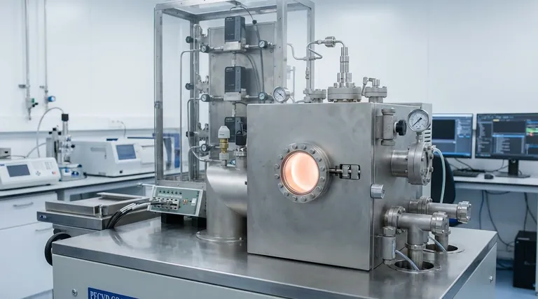
At its core, Chemical Vapor Deposition (CVD) is a highly controlled process used to create a solid, high-performance thin film on a surface, known as a substrate. This is achieved by introducing specific gases, called precursors, into a reaction chamber where they chemically react on the heated substrate's surface. These reactions effectively "build" the new material layer atom by atom, resulting in a thin, uniform coating.
The central principle of CVD is not physical placement, but a chemical transformation. Precursor gases are deliberately chosen to decompose and react at a specific temperature, using the substrate's surface as the foundation to construct a new, solid material layer with precise properties.
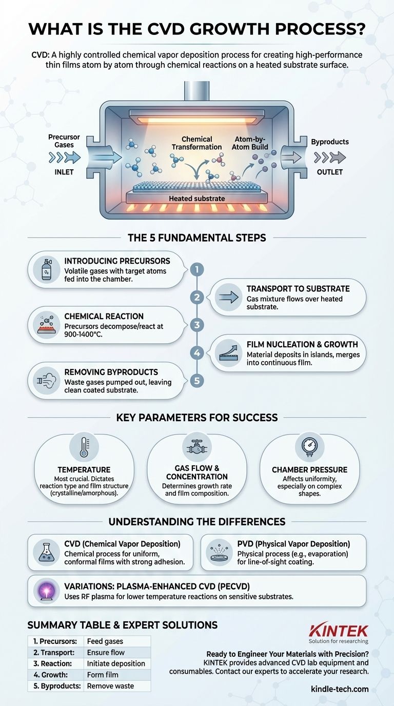
The Fundamental Steps of CVD Growth
The CVD process can be understood as a sequence of carefully controlled events, each playing a critical role in the final quality of the deposited film.
Step 1: Introducing the Precursors
The process begins by feeding one or more volatile precursor gases into a reaction chamber. These gases contain the specific atoms needed for the final film (e.g., carbon-bearing gases to create graphene).
Often, an inert carrier gas is used to dilute the reactants and control their transport to the substrate.
Step 2: Transport to the Substrate
Inside the chamber, the gas mixture flows over one or more substrates, which are arranged to ensure even exposure. The gas molecules diffuse across a boundary layer to reach the substrate surface.
Step 3: The Chemical Reaction
The substrates are heated to a precise temperature, typically between 900-1400 °C, though some variations operate at lower temperatures. This heat provides the necessary energy to trigger a chemical reaction on the surface.
The precursor gases decompose, react with each other, or react with the substrate itself. In some cases, the substrate (like a copper foil for graphene growth) also acts as a catalyst, facilitating the reaction.
Step 4: Film Nucleation and Growth
The chemical reaction deposits solid material onto the substrate. This deposition doesn't happen all at once; it begins at multiple points, forming tiny "islands" of material.
These islands then grow and merge, eventually forming a continuous, solid film across the entire surface.
Step 5: Removing Byproducts
The chemical reactions that form the film also create unwanted gaseous byproducts. These waste gases are carried away from the substrate surface and pumped out of the reaction chamber.
This final step leaves behind only the substrate coated with the newly formed, highly adherent thin film.
Key Parameters That Define the Outcome
The success of CVD hinges on the precise control of several key variables. These parameters directly influence the properties of the final film, such as its thickness, composition, and crystal structure.
The Critical Role of Temperature
Substrate temperature is the most crucial parameter. It dictates which chemical reactions can occur and how fast they happen, directly defining the structure (e.g., crystalline or amorphous) and quality of the deposited film.
Gas Flow and Concentration
The flow rate and concentration of the precursor gases determine the growth rate of the film. Adjusting the gas mixture allows for the creation of films with specific chemical compositions or layered structures.
Pressure within the Chamber
The pressure inside the reaction chamber affects how the gas molecules travel and distribute themselves. Controlling the pressure is essential for achieving uniform film thickness, especially on complex, three-dimensional surfaces.
Understanding the Trade-offs and Variations
Like any advanced technical process, CVD is not a one-size-fits-all solution. Understanding its context and variations is key to its effective application.
CVD vs. PVD (Physical Vapor Deposition)
A common point of confusion is the difference between CVD and PVD. PVD is a physical process, like evaporation or sputtering, that transports a solid material to the substrate without a chemical change.
CVD is a chemical process. This fundamental difference often allows CVD to produce films that are more conformal (able to coat complex shapes evenly) and have stronger adhesion because the film is chemically bonded to the substrate.
Process Variations (e.g., Plasma-Enhanced CVD)
Standard CVD requires very high temperatures, which can damage sensitive substrates like plastics or certain electronic components.
To overcome this, variations like Plasma-Enhanced CVD (PECVD) are used. In PECVD, an RF plasma field is used to energize the precursor gases, allowing the chemical reactions to occur at much lower temperatures.
Substrate and Catalyst Specificity
The choice of substrate is highly intentional. It can be an inert foundation or an active participant. For example, growing graphene via CVD requires a metal catalyst surface (like copper or platinum) to enable the decomposition of carbon gases and the formation of the graphene lattice.
Making the Right Choice for Your Goal
The specific CVD technique you employ should be dictated by the material you are depositing and the nature of your substrate.
- If your primary focus is high-purity, crystalline films (e.g., for semiconductors): Traditional, high-temperature CVD is the gold standard for its precise chemical control and ability to produce highly ordered structures.
- If your primary focus is coating temperature-sensitive materials (e.g., polymers): A low-temperature variant like Plasma-Enhanced CVD (PECVD) is the correct choice to prevent substrate damage.
- If your primary focus is achieving a uniform coating on complex shapes: CVD's gas-phase nature makes it superior to line-of-sight physical methods, ensuring a highly conformal film.
Ultimately, CVD is a powerful and versatile platform for engineering materials from the atom up.
Summary Table:
| CVD Step | Key Action | Purpose |
|---|---|---|
| 1. Introducing Precursors | Feed volatile gases into the chamber | Supply atoms for the final film |
| 2. Transport to Substrate | Gas flows over heated substrate | Ensure even exposure and diffusion |
| 3. Chemical Reaction | Precursors decompose/react on surface | Initiate deposition of solid material |
| 4. Film Nucleation/Growth | Islands of material form and merge | Create a continuous, uniform thin film |
| 5. Removing Byproducts | Waste gases are pumped out | Leave behind a pure, adherent coating |
Ready to Engineer Your Materials with Precision?
KINTEK specializes in providing advanced lab equipment and consumables for Chemical Vapor Deposition and other sophisticated processes. Whether you're developing semiconductors, coatings, or novel materials, our solutions are designed to deliver the precise control and reliability your research demands.
Contact our experts today to discuss how our CVD systems and support can accelerate your innovation and help you achieve superior thin-film results.
Visual Guide
Related Products
- Chemical Vapor Deposition CVD Equipment System Chamber Slide PECVD Tube Furnace with Liquid Gasifier PECVD Machine
- Customer Made Versatile CVD Tube Furnace Chemical Vapor Deposition Chamber System Equipment
- Microwave Plasma Chemical Vapor Deposition MPCVD Machine System Reactor for Lab and Diamond Growth
- 915MHz MPCVD Diamond Machine Microwave Plasma Chemical Vapor Deposition System Reactor
- Custom CVD Diamond Coating for Lab Applications
People Also Ask
- What is plasma enhanced chemical vapor deposition PECVD equipment? A Guide to Low-Temperature Thin Film Deposition
- What types of substrates are used in CVD to facilitate graphene films? Optimize Graphene Growth with the Right Catalyst
- Why is Chemical Vapor Deposition (CVD) equipment uniquely suited for constructing hierarchical superhydrophobic structures?
- What is the chemical vapor deposition growth process? Build Superior Thin Films from the Atom Up
- What are the advantages of chemical vapor deposition? Achieve Superior Thin Films for Your Lab


