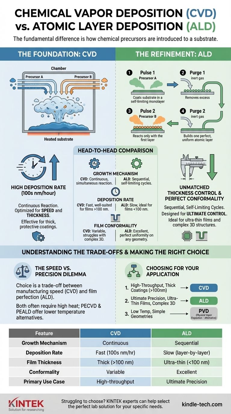
The fundamental difference between Chemical Vapor Deposition (CVD) and Atomic Layer Deposition (ALD) lies in how chemical precursors are introduced to a substrate. In CVD, precursors are delivered simultaneously, creating a continuous reaction that quickly builds a film. In ALD, precursors are introduced in sequential, separate pulses, enabling a self-limiting reaction that builds the film one atomic layer at a time.
While both are chemical deposition methods, CVD is optimized for speed and thickness, whereas ALD is a slower, more precise variant designed for ultimate control over film uniformity and conformality, even on the most complex 3D structures.
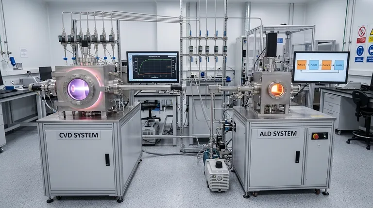
The Foundation: Understanding Chemical Vapor Deposition (CVD)
How CVD Works
Chemical Vapor Deposition is a process where a substrate (or workpiece) is placed inside a reaction chamber and heated.
One or more volatile gaseous chemicals, known as precursors, are then introduced into the chamber. These gases react or decompose on the hot substrate surface, forming a stable solid film and leaving behind volatile byproducts that are removed.
Imagine it as multiple streams of colored paint being sprayed onto a canvas at the same time—the colors mix and build up a layer continuously.
Key Characteristics of CVD
The primary advantage of CVD is its high deposition rate. Because the chemical reactions occur continuously wherever the precursors are present, films can be grown relatively quickly, often at rates of hundreds or thousands of nanometers per hour.
This makes CVD highly effective for creating thick, protective, or functional coatings in industrial applications where throughput is critical.
The Refinement: Atomic Layer Deposition (ALD) as a Sub-Type of CVD
The Self-Limiting Reaction Cycle
ALD is best understood as a precise, sub-class of CVD. Instead of introducing precursors simultaneously, ALD breaks the reaction down into a sequence of distinct, self-limiting steps. A typical two-precursor cycle looks like this:
- Pulse 1: The first precursor gas is pulsed into the chamber. It reacts with the substrate surface until every available reaction site is occupied. No further reaction can occur, making the process self-limiting.
- Purge 1: The chamber is purged with an inert gas to remove all excess precursor molecules.
- Pulse 2: The second precursor gas is pulsed in. It reacts exclusively with the first precursor layer that was just deposited. This reaction is also self-limiting.
- Purge 2: The chamber is purged again to remove unreacted precursors and byproducts, leaving behind exactly one atomic layer of the desired material.
This four-step cycle is repeated hundreds or thousands of times to build a film of the desired thickness.
The Power of Layer-by-Layer Control
This meticulous, cyclical process gives ALD its unique advantages. Because each cycle deposits a single, uniform atomic layer, it provides unmatched thickness control down to the angstrom level.
Furthermore, because the process relies on gaseous diffusion and surface reactions rather than line-of-sight deposition, it achieves perfect conformality. An ALD film will be perfectly uniform in thickness whether it is on a flat surface, deep inside a trench, or coating a complex 3D nanopore.
Head-to-Head Comparison: CVD vs. ALD
Growth Mechanism
CVD: A continuous, simultaneous reaction of multiple precursors. The growth rate is dependent on factors like temperature, pressure, and gas flow. ALD: A sequential, cyclical process with self-limiting surface reactions. Growth is determined solely by the number of cycles performed.
Deposition Rate
CVD: Fast. Well-suited for films from hundreds of nanometers to several microns thick. ALD: Very slow. Ideal for ultra-thin films, typically less than 100 nanometers, where precision is paramount.
Film Conformality
CVD: Variable. Can struggle to coat deep trenches or complex 3D shapes uniformly. ALD: Excellent. Provides a perfectly uniform coating regardless of the substrate's geometry or aspect ratio.
Understanding the Trade-offs
The Speed vs. Precision Dilemma
The choice between CVD and ALD is a classic engineering trade-off between manufacturing speed and film perfection.
CVD delivers high throughput, making it cost-effective for thicker films where minor variations in uniformity are acceptable. ALD delivers unparalleled precision and conformality at the expense of time and, consequently, higher cost per part.
Process Conditions
Both techniques typically require high temperatures to drive the chemical reactions, which can limit the types of substrates that can be used without causing damage or stress.
However, advanced variants like Plasma-Enhanced CVD (PECVD) and Plasma-Enhanced ALD (PEALD) can operate at lower temperatures, broadening their applicability.
Making the Right Choice for Your Application
Choosing the correct method requires a clear understanding of your project's primary goal.
- If your primary focus is high-throughput production or thick coatings (>100 nm): CVD is the superior choice for its speed and cost-effectiveness.
- If your primary focus is ultimate precision on ultra-thin films or perfect uniformity on complex 3D structures: ALD is the necessary technology, especially in advanced microelectronics and nanotechnology.
- If your process requires low temperatures and simple geometries: You may also consider an entirely different category, Physical Vapor Deposition (PVD), which does not rely on chemical reactions.
Ultimately, your application's tolerance for imperfection dictates the right deposition technology.
Summary Table:
| Feature | Chemical Vapor Deposition (CVD) | Atomic Layer Deposition (ALD) |
|---|---|---|
| Growth Mechanism | Continuous, simultaneous reaction | Sequential, self-limiting cycles |
| Deposition Rate | Fast (100s of nm/hour) | Slow (layer-by-layer) |
| Film Thickness | Thick coatings (>100 nm) | Ultra-thin films (<100 nm) |
| Conformality | Variable, struggles with complex 3D shapes | Excellent, perfect uniformity on any geometry |
| Primary Use Case | High-throughput, thick coatings | Ultimate precision, complex 3D structures |
Struggling to choose the right deposition technology for your lab's specific needs? KINTEK specializes in providing lab equipment and consumables for both CVD and ALD processes. Our experts can help you select the perfect solution to achieve the precise film quality, uniformity, and throughput your research or production requires. Contact our team today to discuss your application and discover how KINTEK can enhance your laboratory's capabilities!
Visual Guide
Related Products
- CVD Diamond Dressing Tools for Precision Applications
- Multi Heating Zones CVD Tube Furnace Machine Chemical Vapor Deposition Chamber System Equipment
- CVD Diamond Domes for Industrial and Scientific Applications
- CVD Diamond for Thermal Management Applications
- Chemical Vapor Deposition CVD Equipment System Chamber Slide PECVD Tube Furnace with Liquid Gasifier PECVD Machine
People Also Ask
- What color diamonds are CVD? Understanding the Process from Brown Tint to Colorless Beauty
- What is CVD diamond? The Ultimate Guide to Lab-Grown Diamonds and Their Uses
- Does the chemical vapor deposition be used for diamonds? Yes, for Growing High-Purity Lab Diamonds
- How do you identify a CVD diamond? The Definitive Guide to Lab-Grown Diamond Verification
- What is chemical vapor deposition of diamond? Grow High-Purity Diamonds Atom-by-Atom


