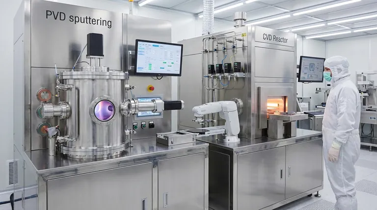
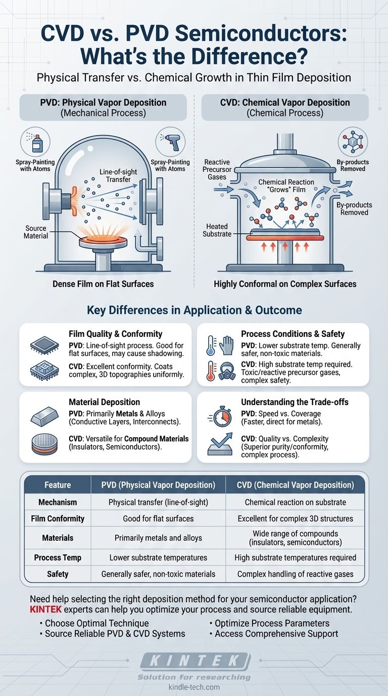
The fundamental difference is that Physical Vapor Deposition (PVD) is a mechanical process, while Chemical Vapor Deposition (CVD) is a chemical one. PVD uses physical forces to transfer a material from a source to a substrate, like spray-painting with atoms. In contrast, CVD uses reactive gases that undergo a chemical reaction directly on the substrate's surface to grow a new layer of material.
While both PVD and CVD are methods for depositing thin films crucial in semiconductor manufacturing, the core distinction lies in their mechanism. PVD is a line-of-sight physical transfer process, whereas CVD is a chemical reaction that "grows" a film, allowing it to conform to complex surfaces.
The Mechanics of Deposition: Physical vs. Chemical
To understand when and why to use each method, we must first look at how they work. The names themselves reveal their core operational principles.
How Physical Vapor Deposition (PVD) Works
PVD is a process of physical transfer conducted in a vacuum. A solid or liquid source material is converted into a vapor through a physical method, such as heating or sputtering.
This vapor then travels in a straight line—a "line-of-sight"—and condenses onto the cooler substrate, forming a dense film. No chemical reactions occur during this deposition.
How Chemical Vapor Deposition (CVD) Works
CVD is a process driven by chemical reactions. Volatile precursor gases, which contain the atoms needed for the film, are introduced into a reaction chamber.
These gases react on the surface of a heated substrate, decomposing to form the desired solid film. Gaseous by-products from the reaction are then removed from the chamber.
Key Differences in Application and Outcome
The choice between PVD and CVD has significant implications for the resulting film's properties, the process conditions, and the types of materials that can be deposited.
Film Quality and Conformity
CVD excels at creating highly conformal films. Because the deposition is based on a chemical reaction that happens everywhere on the surface, it can uniformly coat complex, three-dimensional structures common in modern microchips.
PVD is a line-of-sight process. This makes it excellent for depositing dense films on flat surfaces but can lead to uneven coverage or "shadowing" on intricate topographies.
Process Conditions and Safety
PVD generally does not require heating the substrate itself to high temperatures, though the chamber conditions are hot. It typically uses non-toxic source materials, making the process simpler and safer to handle.
CVD often requires high substrate temperatures to activate and drive the necessary chemical reactions. The precursor gases used can be toxic, corrosive, or flammable, demanding more complex safety and handling protocols.
Material Deposition
PVD is primarily used to deposit elements and some alloys, especially metals for creating conductive layers and interconnects in a chip.
CVD is more versatile for creating compound materials. By carefully selecting precursor gases, it's possible to deposit a wide range of high-purity insulators (like silicon dioxide) and semiconductors (like silicon nitride), which are critical for device performance.
Understanding the Trade-offs
Neither method is universally superior; they are tools designed for different tasks, each with its own set of advantages and limitations.
PVD: Speed vs. Coverage
PVD is often a faster and more direct deposition method, especially for pure metals. Its primary limitation is the line-of-sight nature, which makes it unsuitable for applications requiring perfect, uniform coverage over complex, non-planar surfaces.
CVD: Quality vs. Complexity
CVD provides exceptional film quality, purity, and conformality, which are essential for building high-performance transistors and other micro-scale devices. This quality comes at the cost of process complexity, higher temperatures, and the need to manage chemical reactions and their hazardous by-products.
Making the Right Choice for Your Application
Your final decision depends entirely on the specific layer you are trying to create within the semiconductor device.
- If your primary focus is depositing a pure metal layer for interconnects on a relatively planar surface: PVD is typically the more direct, efficient, and cost-effective choice.
- If your primary focus is growing a high-purity, uniform insulating or semiconducting layer over complex topography: CVD is the superior method for achieving the required quality and conformity.
Ultimately, choosing between these techniques is about selecting the right tool—physical transfer or chemical growth—to build the precise atomic-scale structure you need.
Summary Table:
| Feature | PVD (Physical Vapor Deposition) | CVD (Chemical Vapor Deposition) |
|---|---|---|
| Mechanism | Physical transfer (line-of-sight) | Chemical reaction on substrate |
| Film Conformity | Good for flat surfaces | Excellent for complex 3D structures |
| Materials | Primarily metals and alloys | Wide range of compounds (insulators, semiconductors) |
| Process Temp | Lower substrate temperatures | High substrate temperatures required |
| Safety | Generally safer, non-toxic materials | Complex handling of reactive gases |
Need help selecting the right deposition method for your semiconductor application?
At KINTEK, we specialize in providing advanced lab equipment and consumables for semiconductor manufacturing. Our experts can help you:
• Choose the optimal deposition technique for your specific materials and device requirements • Source reliable PVD and CVD systems that deliver precise, high-quality thin films • Optimize your process parameters for maximum efficiency and performance • Access comprehensive support for installation, maintenance, and troubleshooting
Whether you're working on interconnects, insulators, or complex 3D structures, we have the solutions to enhance your semiconductor fabrication process.
Contact our technical specialists today to discuss your specific needs and discover how KINTEK's semiconductor equipment can accelerate your research and production success.
Visual Guide
Related Products
- Inclined Rotary Plasma Enhanced Chemical Vapor Deposition PECVD Equipment Tube Furnace Machine
- HFCVD Machine System Equipment for Drawing Die Nano-Diamond Coating
- Vacuum Hot Press Furnace Machine for Lamination and Heating
- 915MHz MPCVD Diamond Machine Microwave Plasma Chemical Vapor Deposition System Reactor
- Laboratory CVD Boron Doped Diamond Materials
People Also Ask
- What materials are deposited in PECVD? Discover the Versatile Thin-Film Materials for Your Application
- What is plasma enhanced chemical vapour deposition process? Unlock Low-Temperature, High-Quality Thin Films
- What is PECVD silicon deposition? Achieve Low-Temperature, High-Quality Thin Films
- What is meant by vapor deposition? A Guide to Atomic-Level Coating Technology
- What is the difference between CVD and PECVD? Choose the Right Thin-Film Deposition Method


