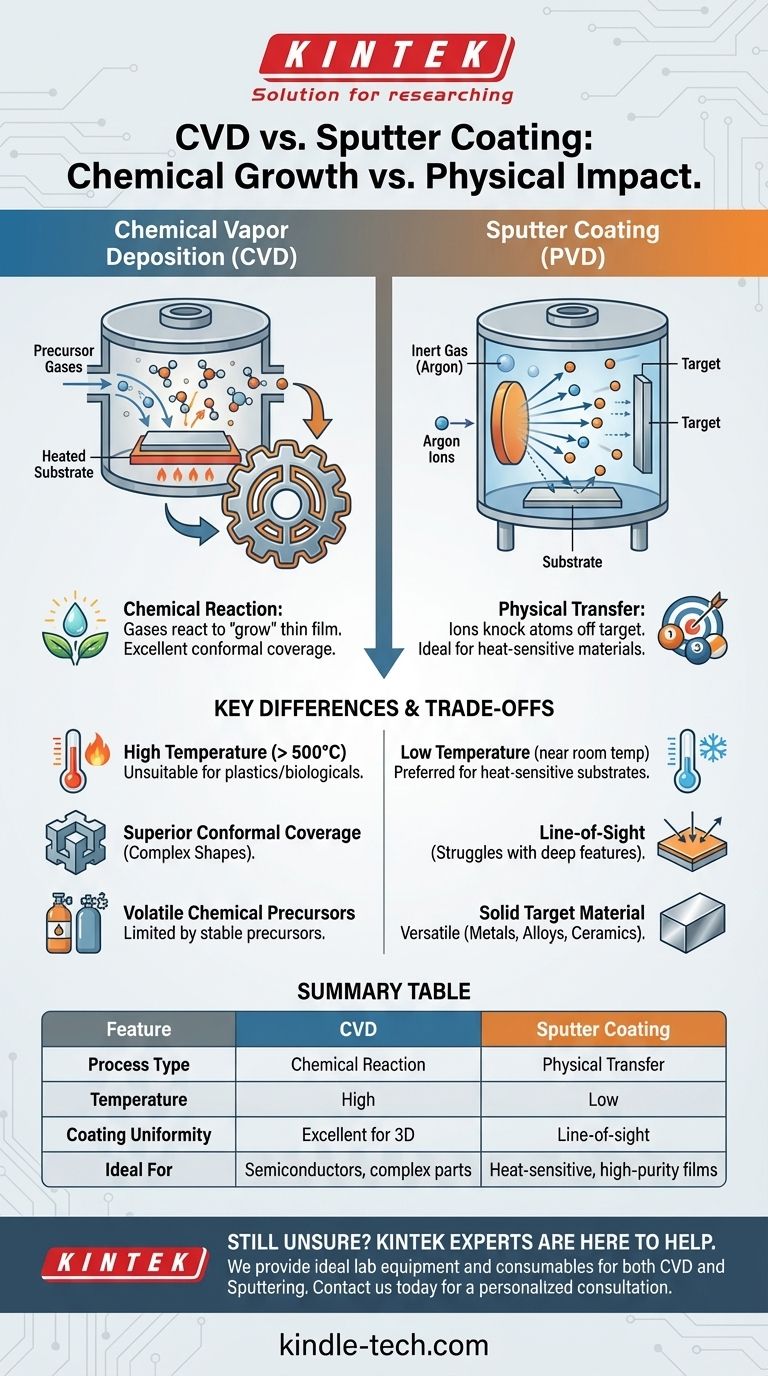
At its core, the difference between Chemical Vapor Deposition (CVD) and Sputter Coating is a matter of chemical reaction versus physical transfer. CVD uses chemical reactions from precursor gases to "grow" a thin film on a surface, much like dew forming on a leaf. Sputtering, a form of Physical Vapor Deposition (PVD), uses high-energy ion bombardment to physically knock atoms off a target material, which then deposit onto the surface like a fine spray.
The fundamental choice between CVD and sputtering is a choice between a chemical process and a physical one. CVD excels at coating complex shapes uniformly but often requires high temperatures, while sputtering is a lower-temperature physical process ideal for heat-sensitive materials and high-purity films.
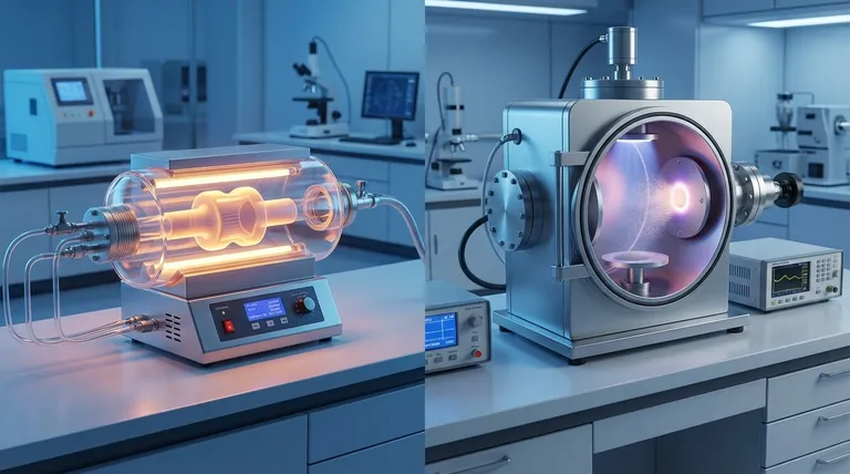
The Core Distinction: Chemical Growth vs. Physical Impact
The mechanism used to move material from a source to your substrate is the most significant differentiator between these two methods. It directly impacts the process parameters and the final film properties.
How CVD Works: Building from Gas
Chemical Vapor Deposition involves introducing volatile precursor gases into a reaction chamber containing the substrate.
When these gases come into contact with the heated substrate, they react or decompose, leaving behind a solid material that forms the desired thin film. For example, solid glucose can be heated to create a carbon vapor that coats a battery component.
This process is not line-of-sight; the gas flows around the object, allowing for a conformal coating that uniformly covers even intricate, three-dimensional shapes and internal channels.
How Sputtering Works: A Billiards Game at the Atomic Scale
Sputtering begins with a solid block of the coating material, known as the target. This target is placed in a vacuum chamber that is backfilled with an inert gas, like argon.
A high voltage is applied, creating a plasma and accelerating the argon ions toward the target. These ions collide with the target with such force that they physically eject or "sputter" atoms of the target material.
These ejected atoms travel through the chamber and deposit onto the substrate, building up the thin film atom by atom.
Understanding the Trade-offs and Key Differences
Your choice between CVD and sputtering depends entirely on the specific requirements of your application, including the substrate material, the desired film properties, and the complexity of the part's geometry.
Temperature: The Deciding Factor for Substrates
CVD processes typically require high temperatures to drive the necessary chemical reactions on the substrate surface. This makes CVD unsuitable for heat-sensitive materials like plastics or many biological samples.
Sputtering, by contrast, is a much lower-temperature process. The substrate can remain at or near room temperature, making it the preferred method for coating heat-sensitive materials.
Coverage and Conformality: Coating Complex Shapes
CVD is the undisputed champion of conformal coverage. Because it relies on a gas that can penetrate small features and internal surfaces, it produces an exceptionally uniform film on even the most complex geometries.
Sputtering is more of a line-of-sight technique. While it can coat three-dimensional objects, it can struggle to uniformly cover deep trenches, sharp corners, or hidden internal surfaces.
Material Source and Film Purity
CVD is limited to materials for which volatile chemical precursors exist and are stable enough to use. The resulting film's purity depends on the efficiency of the reaction and the purity of the precursor gases.
Sputtering is highly versatile and can deposit almost any material that can be fabricated into a solid target, including metals, alloys, and ceramics. It is a very direct transfer of material, often resulting in very high-purity films.
Making the Right Choice for Your Application
Use your primary goal to guide your decision.
- If your primary focus is coating complex 3D parts or internal surfaces uniformly: Choose CVD for its superior conformal coverage.
- If your primary focus is coating a heat-sensitive substrate like plastic: Choose sputtering for its low-temperature physical process.
- If your primary focus is depositing a high-purity metallic or alloy film: Sputtering provides a direct and clean physical transfer of the target material.
- If your primary focus is growing a specific, high-quality crystalline film (e.g., in semiconductors): CVD often provides the precise control over growth conditions necessary for this task.
Understanding whether your application needs a chemical growth process or a physical deposition process is the key to selecting the right technology.
Summary Table:
| Feature | Chemical Vapor Deposition (CVD) | Sputter Coating (PVD) |
|---|---|---|
| Process Type | Chemical reaction from gases | Physical transfer via ion bombardment |
| Temperature | High (often > 500°C) | Low (near room temperature) |
| Coating Uniformity | Excellent for complex 3D shapes | Line-of-sight, may struggle with deep features |
| Ideal For | Semiconductors, complex geometries | Heat-sensitive materials, high-purity metals |
Still unsure which coating method is right for your specific application? The experts at KINTEK are here to help. We specialize in providing the ideal lab equipment and consumables for your thin-film deposition needs, whether you require the high-temperature uniformity of CVD or the low-temperature precision of sputtering. Contact our team today for a personalized consultation and let us help you achieve optimal coating results for your laboratory.
Visual Guide
Related Products
- Custom CVD Diamond Coating for Lab Applications
- HFCVD Machine System Equipment for Drawing Die Nano-Diamond Coating
- Laboratory CVD Boron Doped Diamond Materials
- CVD Diamond for Thermal Management Applications
- CVD Diamond Dressing Tools for Precision Applications
People Also Ask
- What are the different CVD coating? A Guide to Thermal CVD, PECVD, and Specialized Methods
- What are the types of CVD coating? A Guide to Choosing the Right Process
- What is CVD coating used for? Hardening Tools & Building Semiconductors for Industry
- What is CVD diamond coating? Grow a Super-Hard, High-Performance Diamond Layer
- Can you coat something in diamond? Unlock Unmatched Hardness and Thermal Conductivity
