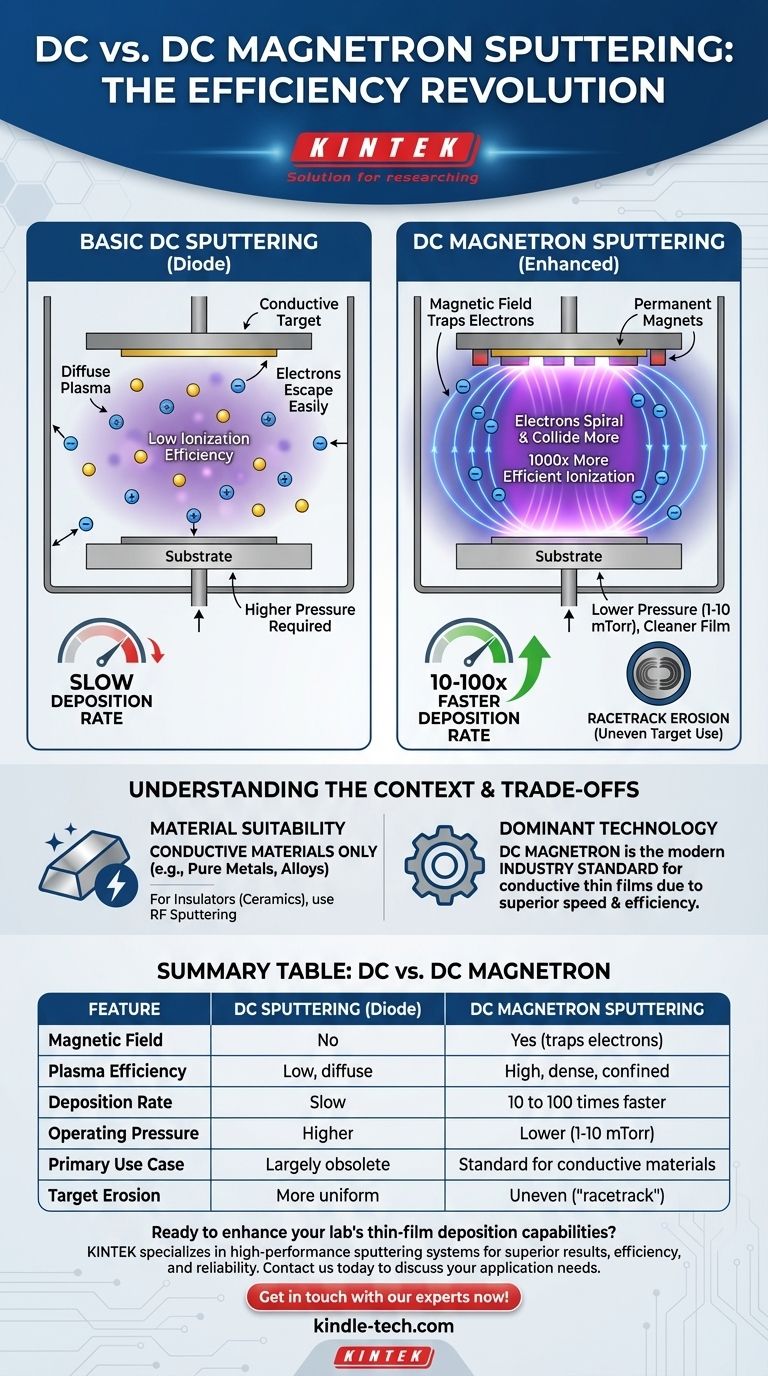
The fundamental difference is the addition of a powerful magnetic field directly behind the target material in DC magnetron sputtering. While both methods use a DC voltage to create a plasma and sputter a target, the magnetron's magnetic field traps electrons near the target surface. This confinement dramatically increases the efficiency of the plasma, leading to significantly higher deposition rates.
At its core, DC magnetron sputtering is not a fundamentally different process, but rather a critical enhancement to basic DC sputtering. The use of magnets solves the primary inefficiency of the original method, making it the modern standard for depositing conductive thin films.

The Foundation: How Basic DC Sputtering Works
The original method, often called DC diode sputtering, is the simplest form of the technology. Understanding its limitations is key to appreciating why the magnetron enhancement was developed.
The Core Process
A high DC voltage is applied between two electrodes in a vacuum chamber filled with an inert gas, typically Argon. The target material (the coating source) acts as the cathode, and the substrate (the object to be coated) is placed on the anode. The voltage ignites the gas into a plasma, creating positively charged Argon ions that are accelerated into the negatively charged target, knocking off atoms that then deposit onto the substrate.
The Primary Limitation: Inefficiency
In this basic setup, the plasma is diffuse and inefficient. Free electrons created in the process can travel directly to the anode or chamber walls without colliding with Argon atoms. This results in a low-density plasma, requiring higher gas pressures to sustain itself, which in turn leads to a slow deposition rate and undesirable heating of the substrate.
The Enhancement: Introducing the Magnetron
DC magnetron sputtering addresses the core inefficiency of the diode method by adding a permanent magnet assembly behind the target cathode.
The Role of the Magnetic Field
This magnetic field projects in a way that traps free electrons in a spiral path directly in front of the target's surface. Instead of escaping, these electrons are forced to travel a much longer distance within the plasma.
The Result: Increased Ionization
The extended path of the trapped electrons drastically increases the probability that they will collide with and ionize neutral Argon atoms. This process is thousands of times more efficient at creating ions than basic DC sputtering.
The Impact on Performance
This hyper-efficient ionization creates a very dense, intense plasma confined to the region directly in front of the target. This dense cloud of ions bombards the target with much greater intensity, resulting in a sputtering rate that is 10 to 100 times higher than basic DC sputtering. This allows the process to be run at lower pressures and voltages.
Understanding the Trade-offs and Context
While DC magnetron sputtering is the dominant technology, it's important to understand its characteristics and where it fits in the broader landscape of sputtering technologies.
Deposition Rate and Efficiency
This is the most significant advantage. DC magnetron sputtering has largely replaced basic DC diode sputtering in nearly all industrial and research applications because of its vastly superior speed and efficiency.
System Pressure and Voltage
Because the magnetic field makes the plasma self-sustaining, magnetron systems can operate at much lower gas pressures (typically 1-10 mTorr). This results in a cleaner deposition environment and higher quality films with less gas incorporation. It also operates at a lower voltage (below 1000V) but higher current.
Target "Racetrack" Erosion
A notable trade-off is that the confined plasma causes uneven erosion of the target material. The area of most intense plasma bombardment forms a distinct groove, often called a "racetrack," which limits the usable portion of the target material.
A Note on Material Type
Both DC and DC magnetron sputtering are only effective for conductive target materials, such as pure metals. If a non-conductive (insulating or dielectric) material like a ceramic is used, the positive ions striking the target will build up a positive charge, eventually neutralizing the voltage and stopping the process. For these materials, Radio Frequency (RF) Sputtering is required.
Making the Right Choice for Your Process
Your choice of sputtering technology is dictated almost entirely by the material you intend to deposit.
- If your primary focus is depositing a conductive film (e.g., metals, alloys): DC Magnetron Sputtering is the modern industry standard due to its high speed, efficiency, and cost-effectiveness.
- If your primary focus is depositing an insulating film (e.g., oxides, nitrides, ceramics): You must use RF Sputtering, which is also almost always enhanced with a magnetron array (becoming RF Magnetron Sputtering) for the same efficiency benefits.
- If you are working with a legacy system or a highly specialized setup: You may encounter basic DC diode sputtering, but it has been almost entirely superseded for practical applications due to its low deposition rate.
Ultimately, the magnetron is the key innovation that transformed sputtering from a slow laboratory technique into a high-throughput, industrial manufacturing process.
Summary Table:
| Feature | DC Sputtering (Diode) | DC Magnetron Sputtering |
|---|---|---|
| Magnetic Field | No | Yes (traps electrons) |
| Plasma Efficiency | Low, diffuse | High, dense, confined |
| Deposition Rate | Slow | 10 to 100 times faster |
| Operating Pressure | Higher | Lower (1-10 mTorr) |
| Primary Use Case | Largely obsolete | Standard for conductive materials |
| Target Erosion | More uniform | Uneven ('racetrack' erosion) |
Ready to enhance your lab's thin-film deposition capabilities?
KINTEK specializes in high-performance sputtering systems and lab equipment. Whether you are depositing conductive metals or require advanced RF solutions for insulating materials, our expertise ensures you get the right equipment for superior results, efficiency, and reliability.
Contact us today to discuss your specific application needs and discover how KINTEK can support your laboratory's success.
Get in touch with our experts now!
Visual Guide
Related Products
- Microwave Plasma Chemical Vapor Deposition MPCVD Machine System Reactor for Lab and Diamond Growth
- Laboratory CVD Boron Doped Diamond Materials
- 915MHz MPCVD Diamond Machine Microwave Plasma Chemical Vapor Deposition System Reactor
- Molybdenum Tungsten Tantalum Special Shape Evaporation Boat
- HFCVD Machine System Equipment for Drawing Die Nano-Diamond Coating
People Also Ask
- How does MPCVD work? A Guide to Low-Temperature, High-Quality Film Deposition
- How are CVD diamonds created? Discover the Science of Lab-Grown Diamond Precision
- Why is argon-rich gas phase chemistry used for UNCD growth? Unlock Precision Nano-Diamond Synthesis
- What pressure is needed for chemical vapor deposition of diamonds? Master the Low-Pressure 'Sweet Spot'
- How does a microwave plasma reactor facilitate the synthesis of diamond? Master MPCVD with Precision Technology


