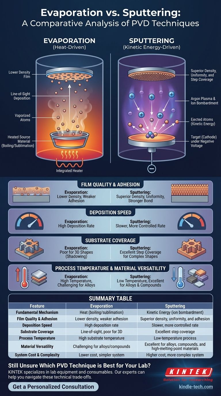
At its core, the difference between evaporation and sputtering lies in how atoms are liberated from a source material to create a thin film. Evaporation uses heat to boil or sublimate a material into a vapor that condenses onto a surface, much like steam fogging a cold mirror. Sputtering, in contrast, uses kinetic energy, where high-energy ions from a plasma bombard a source material, physically knocking atoms off like a cue ball breaking a rack of billiard balls.
While both are physical vapor deposition (PVD) techniques for creating thin films, the choice between them represents a fundamental trade-off: Evaporation offers speed and simplicity, while sputtering delivers superior film quality, adhesion, and uniformity.
The Fundamental Mechanisms: Heat vs. Kinetic Energy
To select the right process, you must first understand how each one works on an atomic level. The methods are fundamentally different, which directly impacts the characteristics of the final film.
How Evaporation Works: Boiling the Source Material
Thermal evaporation is an intuitive process. A source material, or "charge," is placed in a vacuum chamber and heated until it begins to boil or sublimate.
This creates a vapor of atoms that travels through the vacuum. When these vaporized atoms encounter a cooler surface—the substrate—they condense onto it, gradually building up a thin film. The process is "line-of-sight," meaning the material travels in a straight line from the source to the substrate.
How Sputtering Works: A "Billiard Ball" Collision
Sputtering is a more complex, energetic process. It begins by introducing an inert gas, typically argon, into a vacuum chamber and energizing it to create a plasma.
A strong negative voltage is applied to the source material, known as the "target." This attracts the positive argon ions from the plasma, causing them to accelerate and collide with the target at high speed.
These collisions have enough kinetic energy to physically dislodge, or "sputter," atoms from the target. These ejected atoms then travel and deposit onto the substrate, forming a dense and uniform film.
Comparing Key Performance Metrics
The differences in mechanism lead to significant variations in performance, quality, and application suitability.
Film Quality and Adhesion
Sputtering almost always produces a higher-quality film. Sputtered atoms arrive at the substrate with much higher energy than evaporated atoms, creating a denser, more uniform film structure with fewer defects.
This high energy also results in superior adhesion, as the atoms can slightly embed themselves into the substrate surface, forming a stronger bond. Evaporated films are often more porous and can have weaker adhesion.
Deposition Rate and Speed
Evaporation is generally the faster process. By producing a robust vapor stream, evaporation can achieve high deposition rates, making it suitable for high-volume production where cycle time is critical.
Sputtering ejects atoms or small clusters one at a time, which is an inherently slower and more controlled process. This results in lower deposition rates, especially for dielectric materials.
Substrate Coverage and Uniformity
For coating complex, three-dimensional shapes, sputtering is far superior. Sputtered atoms scatter more within the chamber, allowing them to coat sidewalls and intricate features. This is known as good step coverage.
Evaporation's line-of-sight nature creates a "shadowing" effect, making it difficult to achieve a uniform coating on non-flat surfaces.
Understanding the Trade-offs
No single method is universally best. The choice depends on balancing project requirements against the inherent limitations of each technique.
Cost and System Complexity
Evaporation systems are typically simpler and more cost-effective to build and operate. The core components are a vacuum chamber, a power supply for heating, and holders for the source and substrate.
Sputtering systems are more complex, requiring high-voltage power supplies, gas flow controllers, and often magnets (in magnetron sputtering) to increase efficiency. This adds to the initial cost and operational complexity.
Material and Process Control
Sputtering offers greater versatility. It can deposit a wider range of materials, including alloys and compounds, while maintaining their original chemical composition. The process also allows for precise control over film thickness and other properties.
Evaporation can be challenging for materials with very high melting points. When depositing alloys, components with lower boiling points will evaporate first, changing the composition of the resulting film.
Operating Temperature
Sputtering is a lower-temperature process. While the plasma is hot, the substrate itself does not need to be heated and receives less radiant heat from the source. This makes sputtering ideal for coating temperature-sensitive substrates like plastics.
Evaporation requires heating the source material to extremely high temperatures, which can radiate significant heat and potentially damage the substrate.
Making the Right Choice for Your Application
Your final decision must be guided by the primary goal of your project. Each method is a tool optimized for a different set of priorities.
- If your primary focus is high-volume production and low cost: Choose evaporation for its high deposition rates and simpler, more economical system requirements.
- If your primary focus is ultimate film quality, purity, and adhesion: Sputtering is the definitive choice for creating dense, durable, and high-purity films.
- If your primary focus is coating complex 3D shapes or intricate features: Sputtering's superior step coverage is non-negotiable for achieving uniform coating.
- If your primary focus is working with temperature-sensitive substrates or alloys: Sputtering provides the necessary low-temperature operation and compositional control.
Ultimately, selecting the correct deposition method requires a clear understanding of whether your application prioritizes speed and cost or precision and quality.
Summary Table:
| Feature | Evaporation | Sputtering |
|---|---|---|
| Fundamental Mechanism | Heat (boiling/sublimation) | Kinetic energy (ion bombardment) |
| Film Quality & Adhesion | Lower density, weaker adhesion | Superior density, uniformity, and adhesion |
| Deposition Speed | High deposition rate | Slower, more controlled rate |
| Substrate Coverage | Line-of-sight; poor for 3D shapes | Excellent step coverage for complex shapes |
| Process Temperature | High substrate temperature | Low-temperature process |
| Material Versatility | Challenging for alloys/compounds | Excellent for alloys, compounds, and high-melting-point materials |
| System Cost & Complexity | Lower cost, simpler system | Higher cost, more complex system |
Still Unsure Which PVD Technique is Best for Your Lab?
Choosing between evaporation and sputtering is critical for your project's success. The right equipment ensures you achieve the desired film quality, throughput, and cost-efficiency.
KINTEK specializes in lab equipment and consumables, serving laboratory needs. Our experts can help you navigate these technical trade-offs. We provide robust PVD systems and the support you need to optimize your thin film processes.
Contact us today to discuss your specific application requirements. Let KINTEK be your partner in precision.
Get a Personalized Consultation
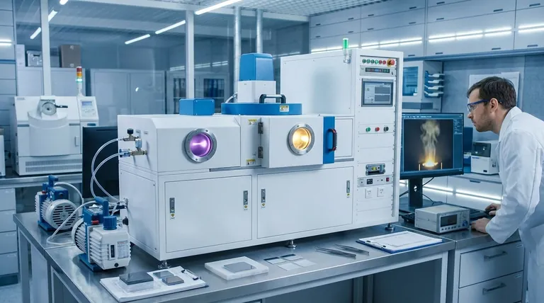
Visual Guide
Related Products
- Spark Plasma Sintering Furnace SPS Furnace
- Vacuum Induction Melting Spinning System Arc Melting Furnace
- Chemical Vapor Deposition CVD Equipment System Chamber Slide PECVD Tube Furnace with Liquid Gasifier PECVD Machine
- Customer Made Versatile CVD Tube Furnace Chemical Vapor Deposition Chamber System Equipment
- Vacuum Cold Mounting Machine for Sample Preparation
People Also Ask
- What technical advantages does a Spark Plasma Sintering (SPS) furnace offer for LZP ceramics? Enhance Ionic Conductivity
- What is the mechanism of SPS process? A Deep Dive into Rapid, Low-Temperature Sintering
- What is the theory of spark plasma sintering? A Guide to Rapid, Low-Temperature Densification
- What is SPS sintering method? A Guide to High-Speed, High-Performance Material Fabrication
- What are the advantages of CAMI/SPS for W-Cu composite preparation? Reduce cycles from hours to seconds.


