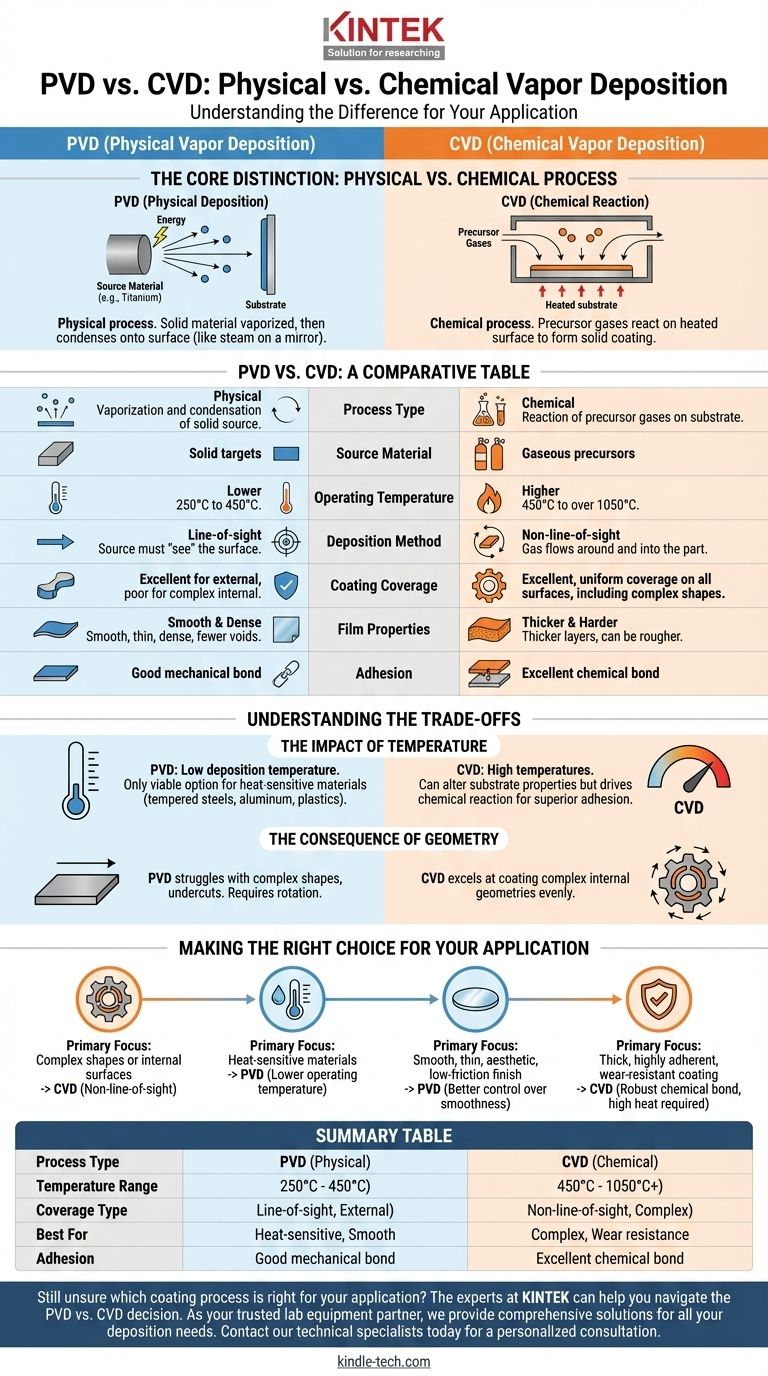
The fundamental difference between Physical Vapor Deposition (PVD) and Chemical Vapor Deposition (CVD) is how the coating material is delivered to the substrate. PVD is a physical process where a solid material is vaporized and then condenses onto a surface, much like steam fogging a cold mirror. In contrast, CVD is a chemical process where precursor gases react on a heated surface to form the solid coating layer.
Your choice between PVD and CVD hinges on a critical trade-off: PVD provides precise, line-of-sight coatings at low temperatures suitable for sensitive parts, while CVD delivers comprehensive, uniform coverage on complex shapes but requires much higher temperatures.
The Core Distinction: Physical vs. Chemical Process
How PVD Works (Physical Deposition)
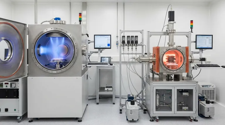
PVD is a "line-of-sight" process. In a high vacuum, a solid source material (like titanium or chromium) is bombarded with energy, causing atoms to physically break off and travel in a straight line.
These vaporized atoms then deposit onto the cooler substrate, forming a thin, dense, and smooth film. Think of it as a highly controlled form of spray painting, but with individual atoms.
How CVD Works (Chemical Reaction)
CVD is not a line-of-sight process. It involves introducing volatile precursor gases into a reaction chamber containing the heated substrate.
The high temperature of the substrate triggers a chemical reaction among the gases, causing a new, solid material to form and deposit uniformly across all exposed surfaces. Because it relies on gas flow, it can easily coat complex internal geometries.
PVD vs. CVD: A Comparative Table
To clarify the practical differences, here is a direct comparison of their key characteristics.
| Characteristic | PVD (Physical Vapor Deposition) | CVD (Chemical Vapor Deposition) |
|---|---|---|
| Process Type | Physical: Vaporization and condensation of a solid source. | Chemical: Reaction of precursor gases on a substrate. |
| Source Material | Solid targets (e.g., metals, ceramics). | Gaseous precursors. |
| Operating Temperature | Lower (250°C to 450°C). | Higher (450°C to over 1050°C). |
| Deposition Method | Line-of-sight: Source must "see" the surface to be coated. | Non-line-of-sight: Gas flows around and into the part. |
| Coating Coverage | Excellent for external surfaces; poor for complex internal geometries. | Excellent, uniform coverage on all exposed surfaces, including complex shapes. |
| Film Properties | Typically very smooth, thin, and dense with fewer voids. | Can produce thicker layers, but may be rougher. |
| Adhesion | Good adhesion, primarily a mechanical bond. | Excellent adhesion due to chemical bonding with the substrate. |
Understanding the Trade-offs
The choice between PVD and CVD is rarely about which is "better" overall, but which is better for a specific application. The differences in their processes create clear trade-offs.
The Impact of Temperature
PVD's key advantage is its relatively low deposition temperature. This makes it the only viable option for coating materials that cannot withstand high heat, such as tempered steels, aluminum alloys, or plastics.
CVD's high temperatures can alter the mechanical properties (like hardness or fatigue life) of the underlying substrate. However, this heat is also what drives the chemical reaction that can lead to superior film adhesion.
The Consequence of Geometry
Because PVD is a line-of-sight process, it struggles to uniformly coat complex shapes with undercuts, holes, or internal passages. The part often needs to be rotated and repositioned to achieve adequate coverage.
CVD excels here. The precursor gases flow around the component, resulting in a highly uniform coating even on the most intricate surfaces, making it ideal for parts like valves or complex tooling.
Film Quality and Application
PVD coatings are known for being exceptionally smooth and dense. This makes them ideal for applications requiring low friction or high aesthetic quality, such as decorative finishes and precision cutting tools.
CVD can produce thicker and harder coatings that are often used for extreme wear resistance. While the surface may not be as smooth as PVD, the robust chemical bond provides outstanding durability in harsh environments.
Making the Right Choice for Your Application
Your final decision must be guided by the specific requirements of your component and its intended use.
- If your primary focus is coating complex shapes or internal surfaces: CVD is the superior choice due to its non-line-of-sight, gas-based deposition.
- If your primary focus is coating heat-sensitive materials: PVD is the definitive solution because of its significantly lower operating temperatures.
- If your primary focus is achieving a very smooth, thin, aesthetic, or low-friction finish: PVD typically offers better control over smoothness and film density.
- If your primary focus is creating a thick, highly adherent coating for extreme wear resistance: CVD is often preferred, provided the substrate can withstand the required heat.
Ultimately, selecting the right deposition method requires a clear understanding of your substrate's limitations and your desired coating's function.
Summary Table:
| Feature | PVD (Physical Vapor Deposition) | CVD (Chemical Vapor Deposition) |
|---|---|---|
| Process Type | Physical vaporization and condensation | Chemical reaction of gases |
| Temperature Range | 250°C - 450°C | 450°C - 1050°C+ |
| Coverage Type | Line-of-sight (external surfaces) | Non-line-of-sight (complex geometries) |
| Best For | Heat-sensitive materials, smooth finishes | Complex shapes, extreme wear resistance |
| Adhesion | Good mechanical bond | Excellent chemical bond |
Still unsure which coating process is right for your application? The experts at KINTEK can help you navigate the PVD vs. CVD decision based on your specific substrate materials, part geometries, and performance requirements. As your trusted lab equipment partner, we provide comprehensive solutions for all your deposition needs.
Contact our technical specialists today for a personalized consultation and discover how KINTEK's expertise in laboratory equipment can optimize your coating processes and enhance your research or manufacturing outcomes.
Visual Guide
Related Products
- Inclined Rotary Plasma Enhanced Chemical Vapor Deposition PECVD Equipment Tube Furnace Machine
- HFCVD Machine System Equipment for Drawing Die Nano-Diamond Coating
- 915MHz MPCVD Diamond Machine Microwave Plasma Chemical Vapor Deposition System Reactor
- Vacuum Hot Press Furnace Machine for Lamination and Heating
- CVD Diamond Cutting Tool Blanks for Precision Machining
People Also Ask
- What is meant by vapor deposition? A Guide to Atomic-Level Coating Technology
- What is the difference between CVD and PECVD? Choose the Right Thin-Film Deposition Method
- What materials are deposited in PECVD? Discover the Versatile Thin-Film Materials for Your Application
- What is PECVD used for? Achieve Low-Temperature, High-Performance Thin Films
- What is plasma enhanced chemical vapour deposition process? Unlock Low-Temperature, High-Quality Thin Films


