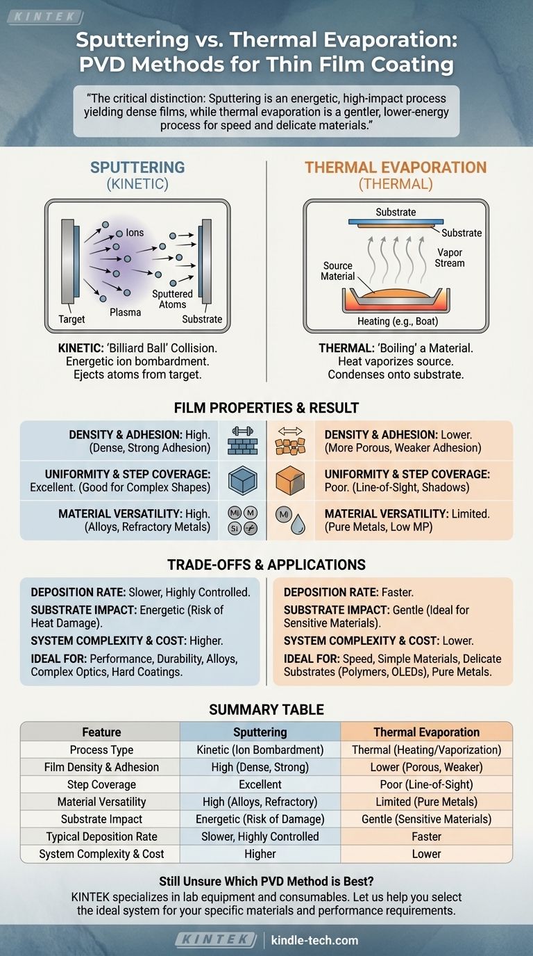
At their core, sputtering and thermal evaporation are two distinct methods of physical vapor deposition (PVD) that achieve the same goal—coating a substrate with a thin film—through fundamentally different physical principles. Sputtering is a kinetic process that uses energetic ion bombardment to physically eject atoms from a target, while thermal evaporation is a thermal process that uses heat to boil a source material into a vapor that then condenses onto the substrate.
The critical distinction is not which method is "better," but understanding the energy involved. Sputtering is an energetic, high-impact process yielding dense and durable films, whereas thermal evaporation is a gentler, lower-energy process ideal for speed and delicate materials.
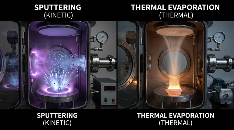
The Fundamental Process: Kinetic vs. Thermal
To choose the right method, you must first understand how each one works. The mechanism directly dictates the properties of the final film.
Sputtering: A Billiard Ball Collision
Sputtering is a physical, momentum-transfer process. Imagine a game of atomic-scale billiards.
First, a vacuum chamber is backfilled with an inert gas, typically Argon. A high voltage is applied, creating a plasma and turning the Argon gas into positively charged ions.
These Argon ions are then accelerated toward the source material, known as the target. When they collide with the target, they physically knock out, or "sputter," atoms of the target material. These ejected atoms then travel through the chamber and deposit onto your substrate, forming a thin film.
Thermal Evaporation: Boiling a Material in a Vacuum
Thermal evaporation is a simpler, more intuitive process analogous to boiling water.
A source material is placed in a high-vacuum chamber inside a container, often a ceramic "boat" or crucible. This material is then heated until it begins to evaporate or sublime, transitioning directly into a gaseous state.
This vapor stream travels in a straight line through the vacuum until it makes contact with the cooler substrate, where it condenses to form a solid thin film. The heating is typically achieved either by passing a large electrical current through the boat (resistive evaporation) or by bombarding the source with a high-energy electron beam (e-beam evaporation).
Comparing the Resulting Thin Film
The differences in these two processes create significant and predictable variations in the final film's characteristics.
Film Density and Adhesion
Sputtered atoms arrive at the substrate with high kinetic energy. This energy allows them to physically impact and embed into the surface, resulting in extremely dense, tightly packed films with superior adhesion.
Evaporated atoms arrive with much lower thermal energy. They tend to "settle" gently onto the substrate, which can lead to more porous films with comparatively weaker adhesion.
Uniformity and Step Coverage
Sputtering generally produces excellent film uniformity over large areas. Because the sputtered atoms scatter more within the chamber, they can coat complex, non-flat surfaces more effectively, a property known as good "step coverage."
Thermal evaporation is largely a "line-of-sight" process. The vapor travels in a straight path from the source to the substrate, which can create "shadows" on components with complex topography and may result in less uniform thickness.
Material Versatility
Sputtering's key advantage is its ability to deposit a vast range of materials. Because it's a physical ejection process, it can deposit alloys (maintaining their composition) and refractory metals with extremely high melting points that are difficult or impossible to evaporate.
Thermal evaporation is limited to materials that can be heated to a vapor phase without decomposing or reacting. It works exceptionally well for pure metals like aluminum, gold, and chromium but is unsuitable for many complex compounds or high-melting-point materials.
Understanding the Trade-offs
Neither technique is universally superior; they represent a classic engineering trade-off between control, speed, and compatibility.
Deposition Rate vs. Process Control
Thermal evaporation, especially e-beam evaporation, can often achieve very high deposition rates, making it efficient for creating thick films quickly.
Sputtering, while sometimes slower, offers exceptionally fine control over film thickness and composition. The process is highly stable and repeatable, making it ideal for complex, multi-layer optical coatings or advanced electronics where precision is paramount.
Potential for Substrate Damage
The high energy inherent in the sputtering process can be a disadvantage. It can transfer significant heat to the substrate and potentially damage sensitive materials like polymers or organic electronic components (OLEDs).
Thermal evaporation is a much "gentler" process from the substrate's perspective. This makes it the default choice for coating temperature-sensitive substrates or devices that could be damaged by ion bombardment.
System Complexity and Cost
Sputtering systems are generally more complex and expensive. They require high-voltage DC or RF power supplies, intricate gas handling and pressure control systems, and often powerful magnets (in magnetron sputtering) to enhance efficiency.
A basic resistive thermal evaporator is one of the simplest and most cost-effective deposition systems available, making it highly accessible for research and straightforward coating applications.
Making the Right Choice for Your Application
Your choice should be dictated entirely by the requirements of your final product.
- If your primary focus is performance and durability: Choose sputtering for its dense, highly adherent films, ideal for optical filters, hard coatings, and high-reliability electronic interconnects.
- If your primary focus is speed with simple materials: Thermal evaporation is an excellent choice for rapidly depositing pure metal films, such as for electrical contacts or basic reflective surfaces.
- If your primary focus is depositing on delicate substrates: The gentle nature of thermal evaporation is essential for working with polymers, organic LEDs (OLEDs), or other temperature-sensitive components.
- If your primary focus is depositing alloys or refractory metals: Sputtering is often the only viable PVD method for materials with very high melting points or for preserving the stoichiometry of complex materials.
Ultimately, selecting the correct deposition method requires matching the unique physics of the process to the desired properties of your film.
Summary Table:
| Feature | Sputtering | Thermal Evaporation |
|---|---|---|
| Process Type | Kinetic (Ion Bombardment) | Thermal (Heating/Vaporization) |
| Film Density & Adhesion | High (Dense, Strong Adhesion) | Lower (More Porous, Weaker Adhesion) |
| Step Coverage | Excellent (Good for Complex Shapes) | Poor (Line-of-Sight, Shadows) |
| Material Versatility | High (Alloys, Refractory Metals) | Limited (Pure Metals, Low Melting Point) |
| Substrate Impact | Energetic (Risk of Heat Damage) | Gentle (Ideal for Sensitive Materials) |
| Typical Deposition Rate | Slower, Highly Controlled | Faster |
| System Complexity & Cost | Higher | Lower |
Still Unsure Which PVD Method is Best for Your Application?
KINTEK specializes in lab equipment and consumables, serving laboratory needs with precision and expertise. Whether you require the dense, durable films of sputtering or the speed and gentleness of thermal evaporation, our team can help you select the ideal system for your specific materials and performance requirements.
Let us help you achieve superior thin film results. Contact our experts today for a personalized consultation and discover how the right PVD technology can enhance your research and development.
Visual Guide