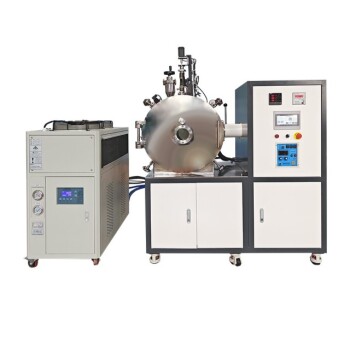
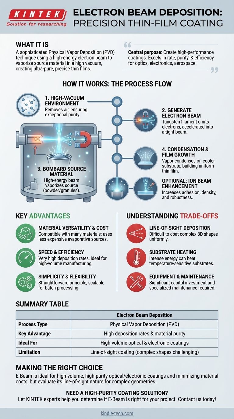
At its core, electron beam deposition is a sophisticated coating technique where a high-energy beam of electrons is used to vaporize a source material inside a high-vacuum chamber. This vaporized material then travels and condenses onto a target object, or substrate, forming an extremely thin and highly pure film. This method is a type of physical vapor deposition (PVD) prized for its precision and control.
The central purpose of electron beam deposition is to create high-performance thin-film coatings. It excels by offering high deposition rates, material purity, and efficiency, making it a cornerstone technology in optics, electronics, and aerospace.

How Electron Beam Deposition Works
To understand why this method is so effective, it's helpful to break down the process into its fundamental stages. Each step is precisely controlled to achieve a specific coating thickness and quality.
The High-Vacuum Environment
The entire process must occur in a high vacuum. This vacuum removes air and other gas molecules that could otherwise react with the vaporized material, ensuring the final coating is exceptionally pure and uncontaminated.
Generating the Electron Beam
A tungsten filament, similar to one in an old-fashioned light bulb, is heated to a very high temperature, causing it to emit a stream of electrons. These electrons are then accelerated and focused into a tight beam using a series of magnetic fields.
Bombarding the Source Material
This high-energy electron beam is directed onto the source material (often in the form of powder or granules) held in a crucible. The intense energy from the beam's impact heats the material, causing it to sublimate or evaporate directly into a gaseous state.
Condensation and Film Growth
The resulting vapor travels in a straight line from the source to the substrate, which is strategically placed within the chamber. Upon contact with the cooler surface of the substrate, the vapor condenses back into a solid, building up layer by layer to form a uniform thin film.
Enhancing the Coating
For applications requiring even greater performance, the process can be augmented with an ion beam. This secondary beam bombards the growing film, increasing the adhesion and creating a denser, more robust coating with less internal stress.
Key Advantages Over Other Methods
Electron beam deposition is not the only way to create thin films, but it holds distinct advantages that make it the preferred choice for certain high-volume and high-purity applications.
Material Versatility and Cost
The method is compatible with a vast array of materials, including metals and dielectrics. Crucially, it can use less expensive evaporative source materials compared to the costly, specially fabricated targets required for other techniques like magnetron sputtering.
Speed and Efficiency
Electron beam deposition can achieve very high deposition rates, meaning it can apply coatings much faster than many alternative methods. This speed makes it ideal for high-volume commercial manufacturing where throughput is a critical factor.
Simplicity and Flexibility
While the equipment is complex, the underlying principle is straightforward and flexible. It is particularly advantageous for creating polymeric coatings and can be scaled effectively for batch processing scenarios.
Understanding the Trade-offs
No single technology is perfect for every situation. To make an informed decision, it's critical to understand the inherent limitations of this process.
Line-of-Sight Deposition
The vaporized material travels in a straight line from the source to the substrate. This "line-of-sight" characteristic means it can be difficult to uniformly coat complex, three-dimensional shapes with undercuts or hidden surfaces.
Substrate Heating
The immense energy required to vaporize the source material can also heat the substrate. For temperature-sensitive materials, this incidental heating can be a significant drawback that may require active cooling or an alternative coating method.
Equipment and Maintenance
The high-vacuum pumps, high-voltage electron gun, and magnetic guidance systems represent a significant capital investment. This complex equipment also requires specialized maintenance to ensure consistent and reliable operation.
Making the Right Choice for Your Goal
Selecting the correct deposition method depends entirely on the priorities of your project.
- If your primary focus is high-volume production of optical or electronic coatings: E-Beam is an excellent choice due to its high deposition rates, material purity, and precision control over film thickness.
- If your primary focus is minimizing material costs: The ability to use a wide range of less expensive raw evaporative materials makes E-Beam highly attractive compared to sputtering.
- If your primary focus is coating complex 3D geometries uniformly: You should carefully evaluate whether E-Beam's line-of-sight nature will meet your needs or if a more conformal method is required.
By weighing these factors, you can determine if the unique combination of speed, purity, and versatility offered by electron beam deposition aligns with your specific engineering and manufacturing goals.
Summary Table:
| Feature | Electron Beam Deposition |
|---|---|
| Process Type | Physical Vapor Deposition (PVD) |
| Key Advantage | High deposition rates & material purity |
| Ideal For | High-volume optical & electronic coatings |
| Limitation | Line-of-sight coating (complex shapes can be challenging) |
Need a high-purity coating solution for your lab?
Electron beam deposition is a powerful technique for creating precise, high-performance thin films. At KINTEK, we specialize in providing the advanced lab equipment and expert support that laboratories need to achieve superior results in optics, electronics, and materials science.
Let our experts help you determine if E-Beam deposition is right for your project. Contact us today to discuss your specific application and requirements!
Visual Guide
Related Products
- Inclined Rotary Plasma Enhanced Chemical Vapor Deposition PECVD Equipment Tube Furnace Machine
- HFCVD Machine System Equipment for Drawing Die Nano-Diamond Coating
- 915MHz MPCVD Diamond Machine Microwave Plasma Chemical Vapor Deposition System Reactor
- Vacuum Hot Press Furnace Machine for Lamination and Heating
- Laboratory Sterilizer Lab Autoclave Pulse Vacuum Lifting Sterilizer
People Also Ask
- What is meant by vapor deposition? A Guide to Atomic-Level Coating Technology
- What is the difference between PECVD and CVD? Unlock the Right Thin-Film Deposition Method
- What is plasma enhanced chemical vapour deposition process? Unlock Low-Temperature, High-Quality Thin Films
- How does plasma enhanced CVD work? Achieve Low-Temperature, High-Quality Thin Film Deposition
- What is plasma in CVD process? Lowering Deposition Temperatures for Heat-Sensitive Materials