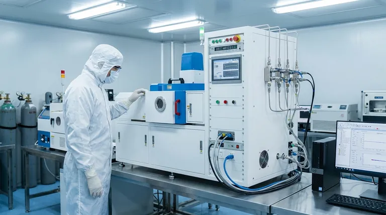
In semiconductor manufacturing, film deposition is the fundamental process of applying a thin, highly controlled layer of material onto a silicon wafer. This is not simply a coating; it is an atomic-level construction process that builds the functional layers of a microchip. The two principal methods for achieving this are Chemical Vapor Deposition (CVD) and Physical Vapor Deposition (PVD).
The core challenge of film deposition is to transform a source material into a vapor, transport it, and have it condense or react on a wafer's surface to form a perfectly uniform and pure solid layer. The choice between chemical methods (CVD) and physical methods (PVD) depends entirely on the specific material being deposited and its role in the final integrated circuit.
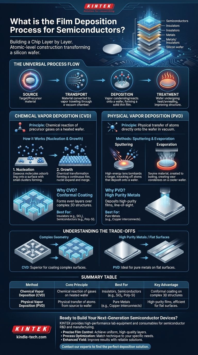
The Goal: Building a Chip Layer by Layer
Before diving into the methods, it's crucial to understand why these films are necessary. A modern microprocessor is built like a skyscraper, with dozens of intricate layers stacked on top of a silicon foundation.
What is a "Thin Film"?
A thin film is a layer of material ranging from a few nanometers to several micrometers in thickness. Each film serves a specific purpose, acting as a conductor (like copper wiring), an insulator (like silicon dioxide), or a semiconductor (the active part of a transistor).
The Universal Process Flow
Regardless of the specific technique, all deposition processes follow a similar high-level sequence:
- Source: A pure source material (known as a target or precursor) is chosen.
- Transport: This material is converted into a vapor state and transported to the wafer, typically within a vacuum chamber.
- Deposition: The vaporized material deposits onto the substrate (the wafer), forming the solid thin film.
- Treatment: The film may undergo heat treatment (annealing) to improve its crystalline structure and properties.
Chemical Vapor Deposition (CVD): Building with Reactions
CVD is the most widely used deposition method in the semiconductor industry due to its unparalleled precision and ability to create highly uniform layers.
The Core Principle of CVD
Instead of physically moving the final material, CVD uses a chemical reaction. Precursor gases are introduced into a chamber containing the heated wafer. These gases react on the hot surface, depositing the desired solid material and leaving behind volatile byproducts that are pumped away.
How a CVD Process Works
The process can be understood through two key stages: nucleation and growth.
- Nucleation: Gaseous precursor molecules are adsorbed onto the wafer surface.
- Growth: These molecules undergo a chemical transformation, forming a solid nucleus of the desired material. These nuclei expand and merge, eventually forming a continuous, high-quality film.
Why CVD is an Industry Workhorse
CVD's primary advantage is its ability to produce conformal coatings. Because the deposition is driven by a chemical reaction, the film forms evenly over complex, three-dimensional structures on the wafer, which is essential for modern transistor architecture.
Physical Vapor Deposition (PVD): Moving Matter Directly
PVD encompasses a set of techniques that physically move atoms from a source material directly onto the wafer's surface. This is done in a high-vacuum environment to ensure purity.
The Core Principle of PVD
PVD is fundamentally a line-of-sight process. Think of it as an atomic-level spray paint, where individual atoms are ejected from a source and travel in a straight line to coat the substrate.
The Sputtering Method
Sputtering is the most common PVD technique. It involves bombarding a solid target of the source material with high-energy ions (typically argon). This collision physically knocks atoms off the target, which then travel and deposit onto the wafer.
The Evaporation Method
Another PVD technique is evaporation. In this process, the source material is heated in a vacuum until it boils, creating a vapor. This vapor then travels to the cooler wafer and condenses on its surface, forming the thin film.
Understanding the Trade-offs
The choice between CVD and PVD is not about which is "better" but which is right for the specific layer being built.
CVD's Strength: Complex Geometry
CVD excels at creating uniform, conformal layers of insulators (like silicon dioxide) and semiconductors (like polycrystalline silicon). Its chemical nature allows it to coat the inside of deep trenches and over complex topography evenly.
PVD's Strength: High Purity Metals
PVD is the go-to method for depositing pure metals, which are used for the wiring (interconnects) on a chip. Because it's a physical process, it can deposit materials that are difficult to create through chemical reactions. Its main limitation is poor performance on complex surfaces, as it struggles to coat "shadowed" areas.
The Deciding Factor: The Layer's Function
The decision hinges on the material required and the wafer's surface topography. Insulators need to cover everything perfectly, making CVD ideal. Metal interconnects require high purity and are often deposited on flatter surfaces, making PVD the more efficient choice.
Matching the Process to Your Goal
To build a functional device, engineers use a combination of these techniques, choosing the right tool for each specific layer.
- If your primary focus is creating a high-quality, uniform insulating layer over a complex surface: CVD is the definitive choice for its superior conformal coating capabilities.
- If your primary focus is depositing a pure metal film for electrical wiring: PVD, especially sputtering, is the industry standard due to its speed, purity, and control.
- If your primary focus is growing a perfect crystalline semiconductor layer: Advanced, highly-controlled CVD techniques are required to manage the precise nucleation and growth of the film.
Ultimately, these deposition processes are the essential construction techniques that transform a blank silicon wafer into a powerful and complex integrated circuit.
Summary Table:
| Method | Core Principle | Best For | Key Advantage |
|---|---|---|---|
| Chemical Vapor Deposition (CVD) | Chemical reaction of gases on a heated wafer surface. | Insulators, Semiconductors (e.g., SiO₂, Poly-Si) | Conformal coating on complex 3D structures. |
| Physical Vapor Deposition (PVD) | Physical transfer of atoms from a source to the wafer. | Pure Metals (e.g., Copper interconnects) | High-purity films, efficient for flat surfaces. |
Ready to Build Your Next-Generation Semiconductor Devices?
Choosing the right deposition process is critical for your lab's success. KINTEK specializes in providing high-performance lab equipment and consumables for semiconductor R&D and manufacturing.
We help you achieve:
- Precise Film Control: Access the right tools for CVD or PVD to build uniform, high-quality layers.
- Process Optimization: Get the equipment and support to match the deposition technique to your specific material and structural goals.
- Enhanced Yield: Improve your results with reliable, industry-standard solutions.
Let's discuss your semiconductor fabrication needs. Contact our experts today to find the perfect deposition solution for your laboratory.
Visual Guide
Related Products
- Chemical Vapor Deposition CVD Equipment System Chamber Slide PECVD Tube Furnace with Liquid Gasifier PECVD Machine
- RF PECVD System Radio Frequency Plasma-Enhanced Chemical Vapor Deposition RF PECVD
- Microwave Plasma Chemical Vapor Deposition MPCVD Machine System Reactor for Lab and Diamond Growth
- Customer Made Versatile CVD Tube Furnace Chemical Vapor Deposition Chamber System Equipment
- CVD Diamond for Thermal Management Applications
People Also Ask
- What happens during deposition chemistry? Building Thin Films from Gaseous Precursors
- How are carbon nanotubes grown? Master Scalable Production with Chemical Vapor Deposition
- How expensive is chemical vapor deposition? Understanding the True Cost of High-Performance Coating
- What are the core advantages of PE-CVD in OLED encapsulation? Protect Sensitive Layers with Low-Temp Film Deposition
- What are the processes of vapor phase deposition? Understand CVD vs. PVD for Superior Thin Films


