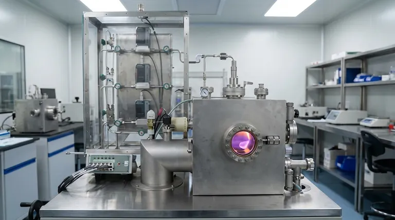
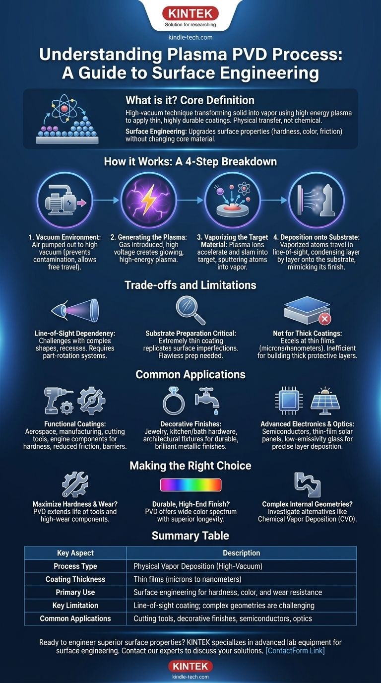
At its core, the Plasma Physical Vapor Deposition (PVD) process is a high-vacuum technique for applying an exceptionally thin yet highly durable coating to a material. It works by transforming a solid coating material into a vapor using a high-energy plasma, which then travels through the vacuum and condenses onto the target object, building the new surface atom by atom. This method is not a chemical reaction but a purely physical transfer of material.
PVD is best understood not as a simple coating, but as a form of surface engineering. It allows you to fundamentally upgrade the surface properties of a substrate—like its hardness, color, or friction—without changing the core material itself.
How Does Plasma PVD Work? A Step-by-Step Breakdown
The PVD process takes place inside a sealed vacuum chamber and can be broken down into four critical stages. Each step is precisely controlled to achieve the desired film properties.
The Vacuum Environment
First, the object to be coated (the substrate) and the solid coating material (the target) are placed inside a chamber. Almost all the air is pumped out to create a high vacuum, which prevents contamination from atmospheric gases and allows vaporized atoms to travel freely.
Generating the Plasma
Next, a gas (typically an inert one like Argon) is introduced into the chamber. A high-power electrical voltage is applied, which strips electrons from the gas atoms and creates a glowing, high-energy state of matter known as plasma.
Vaporizing the Target Material
The positively charged ions within this plasma are accelerated by the electric field and slam into the negatively charged target material. This high-energy bombardment is powerful enough to knock individual atoms or small clusters of atoms loose from the target, a process known as sputtering. These vaporized atoms are now free to travel within the chamber.
Deposition onto the Substrate
The vaporized atoms from the target travel in a straight line through the vacuum until they strike the substrate. Upon contact, they condense back into a solid state, forming a thin, dense, and highly adherent film that builds up layer by layer. The result is a coating that perfectly mimics the substrate's surface finish.
Understanding the Trade-offs and Limitations
While PVD is a powerful technology, it is not the solution for every application. Understanding its inherent limitations is key to making an informed decision.
Line-of-Sight Dependency
The PVD process is fundamentally line-of-sight. The vaporized atoms travel in a straight line from the target to the substrate. This makes it challenging to evenly coat complex shapes with deep recesses, holes, or internal surfaces without sophisticated part-rotation systems.
Substrate Preparation is Critical
The final PVD coating is extremely thin and will precisely replicate the texture of the surface it is applied to. Any imperfections, scratches, or blemishes on the substrate will be visible in the final product. Achieving a high-quality finish requires a flawlessly prepared surface.
Not Ideal for Thick Coatings
PVD excels at creating very thin films, typically measured in microns or even nanometers. While extremely durable for their thickness, the process is not efficient for building up thick protective layers, where processes like thermal spray or electroplating might be more suitable.
Common Applications: Where PVD Shines
PVD's unique combination of durability and precision makes it invaluable across a wide range of industries for both functional and aesthetic purposes.
Functional Coatings
In aerospace and manufacturing, PVD is used to enhance the hardness and reduce the friction of cutting tools, drills, and engine components. It also creates diffusion barriers that protect parts from high temperatures and chemical attack.
Decorative Finishes
PVD provides durable and brilliant metallic finishes for consumer products. It is widely used on jewelry, kitchen and bathroom hardware, and architectural fixtures to create a finish that is far more resistant to scratches and tarnishing than traditional plating.
Advanced Electronics and Optics
The precision of PVD is essential in manufacturing semiconductors, thin-film solar panels, and low-emissivity glass coatings. It allows for the deposition of specific layers that control the flow of electricity or the reflection and transmission of light.
Making the Right Choice for Your Project
Choosing a surface treatment requires aligning the technology's capabilities with your primary goal.
- If your primary focus is maximum surface hardness and wear resistance: PVD is an excellent choice for extending the life of tools and high-wear mechanical components.
- If your primary focus is a durable, high-end decorative finish: PVD offers a wide spectrum of colors with superior longevity compared to most other finishing methods.
- If your primary focus is coating complex internal geometries: You should investigate alternative processes like Chemical Vapor Deposition (CVD), which uses a gas that can penetrate and coat non-line-of-sight surfaces.
Ultimately, plasma PVD empowers you to engineer the precise surface performance your product demands.
Summary Table:
| Key Aspect | Description |
|---|---|
| Process Type | Physical Vapor Deposition (High-Vacuum) |
| Coating Thickness | Thin films (microns to nanometers) |
| Primary Use | Surface engineering for hardness, color, and wear resistance |
| Key Limitation | Line-of-sight coating; complex geometries are challenging |
| Common Applications | Cutting tools, decorative finishes, semiconductors, optics |
Ready to engineer superior surface properties for your products? The plasma PVD process can provide the durable, high-performance coatings your laboratory or manufacturing operation needs. KINTEK specializes in advanced lab equipment and consumables for surface engineering applications. Contact our experts today to discuss how our solutions can help you achieve precise, reliable coatings for tools, components, and consumer goods.
Visual Guide
Related Products
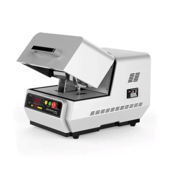
- Inclined Rotary Plasma Enhanced Chemical Vapor Deposition PECVD Equipment Tube Furnace Machine
- Vacuum Hot Press Furnace Machine for Lamination and Heating
- 915MHz MPCVD Diamond Machine Microwave Plasma Chemical Vapor Deposition System Reactor
- Laboratory Sterilizer Lab Autoclave Pulse Vacuum Lifting Sterilizer
- HFCVD Machine System Equipment for Drawing Die Nano-Diamond Coating
People Also Ask
- What is PECVD silicon deposition? Achieve Low-Temperature, High-Quality Thin Films
- What is plasma enhanced chemical vapour deposition process? Unlock Low-Temperature, High-Quality Thin Films
- What is the difference between CVD and PECVD? Choose the Right Thin-Film Deposition Method
- What is plasma in CVD process? Lowering Deposition Temperatures for Heat-Sensitive Materials
- What is meant by vapor deposition? A Guide to Atomic-Level Coating Technology