At its core, the principle of Metal-Organic Chemical Vapor Deposition (MOCVD) is a highly-controlled process for growing high-purity, crystalline thin films. It works by introducing specific gas molecules, known as metal-organic precursors, into a reaction chamber where they decompose on a heated substrate. This chemical reaction meticulously deposits a thin solid film, atom by atom, forming a perfect crystal structure essential for high-performance electronic and photonic devices.
The central challenge in advanced manufacturing is not just depositing material, but building flawless, single-crystal layers on a substrate. MOCVD solves this by using volatile chemical precursors that are designed to react and break apart only at the hot surface of the substrate, enabling a precise and scalable method for creating epitaxial films.
Deconstructing the MOCVD Process
MOCVD is a specialized sub-class of a broader technology known as Chemical Vapor Deposition (CVD). Understanding the general principle of CVD is the first step to mastering the specifics of MOCVD.
The Foundation: Chemical Vapor Deposition (CVD)
In any CVD process, reactive gases are passed over a heated substrate. The heat provides the energy needed to trigger a chemical reaction. This reaction causes a solid material to form and deposit onto the substrate surface, while any unwanted byproducts are removed by the gas flow.
The "MO" in MOCVD: Metal-Organic Precursors
What makes MOCVD unique are the specific source gases it uses. These are metal-organic precursors, which are molecules containing a desired metal atom (like Gallium, Indium, or Aluminum) chemically bonded to organic molecular groups.
The critical property of these precursors is their volatility. They can be easily turned into a vapor at low temperatures, allowing them to be transported precisely using a carrier gas.
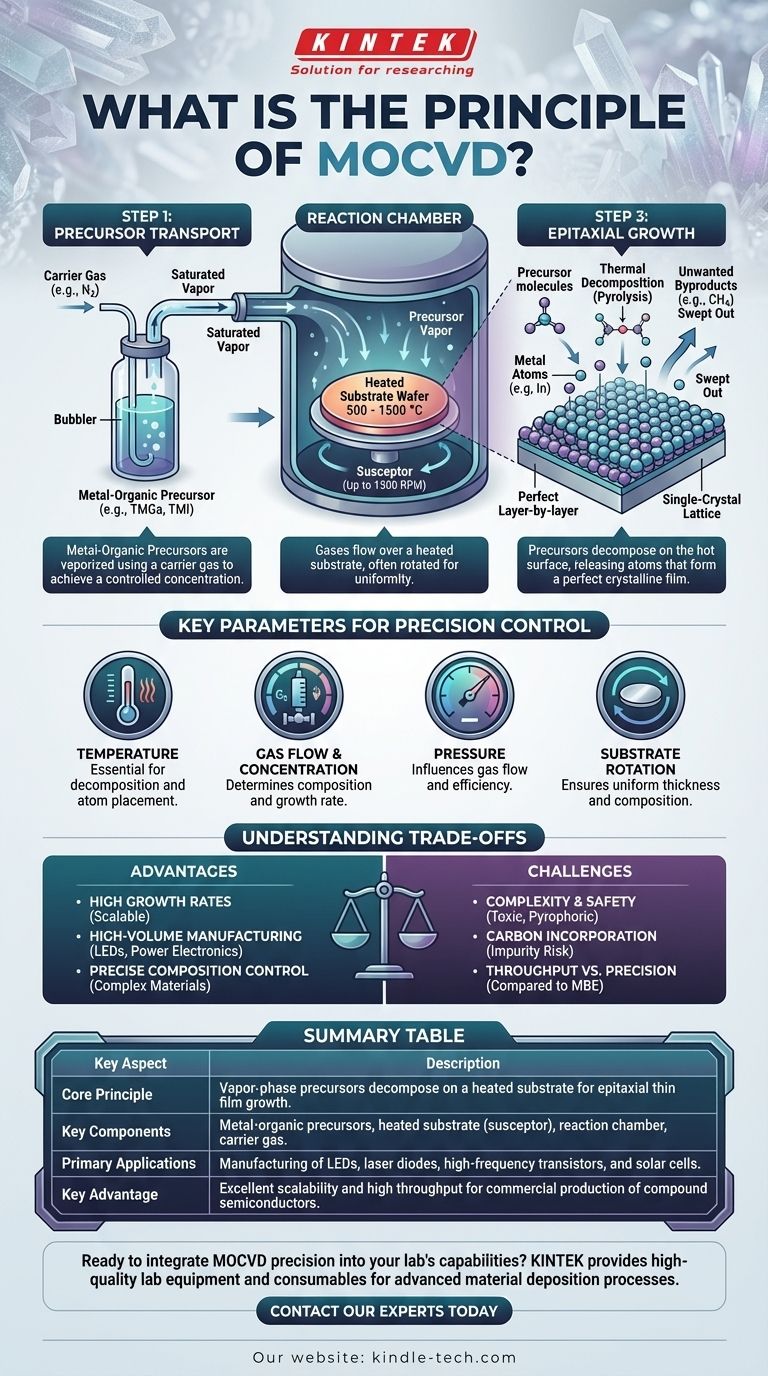
Step 1: Precursor Transport
The process begins by transporting the precursors to the reactor. This is often done using a device called a bubbler.
A carrier gas (such as hydrogen or nitrogen) is bubbled through the liquid metal-organic source. As it bubbles, it becomes saturated with the precursor vapor, carrying a controlled concentration of the reactive material into the reaction chamber.
Step 2: The Reaction Chamber
Inside the chamber, a substrate wafer sits on a heated platform, known as a susceptor. Substrate temperatures are high, typically ranging from 500 to 1500 degrees Celsius.
The precursor gases, mixed with other necessary reactants, are injected into the chamber and flow uniformly across the heated substrate. To ensure this uniformity, the substrate is often rotated at high speeds.
Step 3: Surface Reaction and Epitaxial Growth
When the hot precursors touch the much hotter substrate, they undergo pyrolysis, or thermal decomposition. The chemical bonds break.
The desired metal atoms are released and deposit onto the substrate surface. Because the substrate is a single crystal, the deposited atoms arrange themselves to follow its existing crystal lattice, extending the structure perfectly. This layer-by-layer replication is called epitaxial growth.
The leftover organic components and other byproducts remain in a gaseous state and are swept out of the chamber, leaving behind a pure, crystalline thin film.
The Key Parameters for Precision Control
The quality and properties of the film grown via MOCVD depend on the rigorous control of several process variables. These are monitored in real-time to ensure reproducibility and performance.
Temperature
Temperature is the primary driver of the chemical reaction. It must be high enough to efficiently decompose the precursors but optimized to ensure the atoms have enough energy to find their proper place in the crystal lattice, minimizing defects.
Gas Flow and Concentration
The flow rate of the carrier gas through the bubbler, along with the bubbler's temperature, precisely determines the concentration of reactants delivered to the chamber. This directly controls the film's chemical composition and its growth rate.
Pressure
MOCVD is often performed at pressures ranging from low vacuum to near-atmospheric pressure. The pressure inside the chamber influences the gas flow dynamics and the mean free path of molecules, affecting the uniformity and efficiency of the deposition process.
Substrate Rotation
Rotating the substrate at speeds up to 1500 RPM is crucial for large-scale production. It averages out any minor variations in temperature or gas flow across the wafer, ensuring the resulting film has a highly uniform thickness and composition.
Understanding the Trade-offs
While powerful, MOCVD is not without its challenges. Understanding its limitations is key to using it effectively.
Complexity and Safety
The metal-organic precursors are often highly toxic, flammable, and pyrophoric (igniting spontaneously on contact with air). Consequently, MOCVD reactors require sophisticated gas handling and safety-interlock systems, adding to their complexity and cost.
Carbon Incorporation
Because the precursors contain organic (carbon-based) groups, there is a risk that stray carbon atoms can be incorporated into the growing film as an impurity. This can negatively impact the material's electronic or optical properties, and process conditions must be carefully tuned to minimize it.
Throughput vs. Precision
Compared to ultra-high vacuum techniques like Molecular Beam Epitaxy (MBE), MOCVD offers significantly higher growth rates and is more easily scaled to handle multiple wafers at once. This makes it the dominant choice for high-volume manufacturing. The trade-off is that MBE can, in some specific research applications, offer even finer control at the single-atomic-layer level.
Making the Right Choice for Your Goal
The decision to use MOCVD is driven by the need for high-quality crystalline materials, often at a commercial scale.
- If your primary focus is high-volume manufacturing of compound semiconductors: MOCVD is the industry standard for creating LEDs, laser diodes, and power electronics due to its high throughput and scalability.
- If your primary focus is growing complex material systems with precise composition: MOCVD provides excellent control over doping and alloy composition, making it ideal for materials like Gallium Nitride (GaN) or Gallium Arsenide (GaAs).
- If your primary focus is balancing quality with production efficiency: MOCVD represents the optimal balance between achieving high-quality epitaxial growth and the practical demands of manufacturing.
Ultimately, the principle of MOCVD provides a powerful and scalable chemical toolkit for building the crystalline foundation of next-generation electronic and photonic devices.
Summary Table:
| Key Aspect | Description |
|---|---|
| Core Principle | Vapor-phase precursors decompose on a heated substrate for epitaxial thin film growth. |
| Key Components | Metal-organic precursors, heated substrate (susceptor), reaction chamber, carrier gas. |
| Primary Applications | Manufacturing of LEDs, laser diodes, high-frequency transistors, and solar cells. |
| Key Advantage | Excellent scalability and high throughput for commercial production of compound semiconductors. |
Ready to integrate MOCVD precision into your lab's capabilities?
KINTEK specializes in providing high-quality lab equipment and consumables for advanced material deposition processes like MOCVD. Whether you are scaling up production or pushing the boundaries of R&D, our expertise ensures you have the reliable tools needed for success.
Contact our experts today to discuss how our solutions can enhance your thin film research and manufacturing.
Visual Guide
Related Products
- Multi Heating Zones CVD Tube Furnace Machine Chemical Vapor Deposition Chamber System Equipment
- 915MHz MPCVD Diamond Machine Microwave Plasma Chemical Vapor Deposition System Reactor
- Microwave Plasma Chemical Vapor Deposition MPCVD Machine System Reactor for Lab and Diamond Growth
- Cylindrical Resonator MPCVD Machine System Reactor for Microwave Plasma Chemical Vapor Deposition and Lab Diamond Growth
- Molybdenum Vacuum Heat Treat Furnace
People Also Ask
- What is a CVD tube furnace? A Complete Guide to Thin-Film Deposition
- What is the function of a high-temperature CVD tube furnace in 3D graphene foam prep? Master 3D Nanomaterial Growth
- What method is used to grow graphene? Master High-Quality Production with CVD
- What is the function of a tube furnace in CVD SiC synthesis? Achieving Ultra-Pure Silicon Carbide Powders
- What is the difference between hot wall CVD and cold wall CVD? Choose the Right System for Your Process