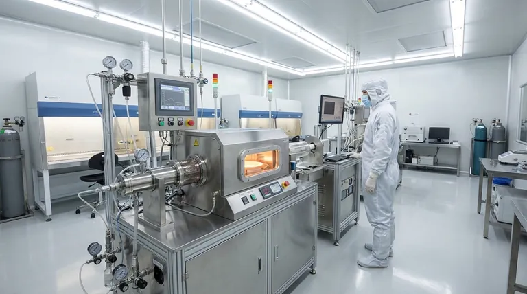
In essence, Chemical Vapor Deposition (CVD) is a manufacturing process that builds a high-purity, solid thin film on a surface, known as a substrate. It accomplishes this by introducing carefully selected precursor gases into a reaction chamber. These gases then chemically react near or on the heated substrate, and the resulting solid material is deposited onto it, forming the desired layer.
The core principle of CVD is not merely condensation; it is a controlled chemical reaction in a gaseous state that "grows" a solid material onto a wafer. This method is fundamental to modern semiconductor fabrication because it allows for the precise deposition of a wide variety of materials, from insulators to conductors.
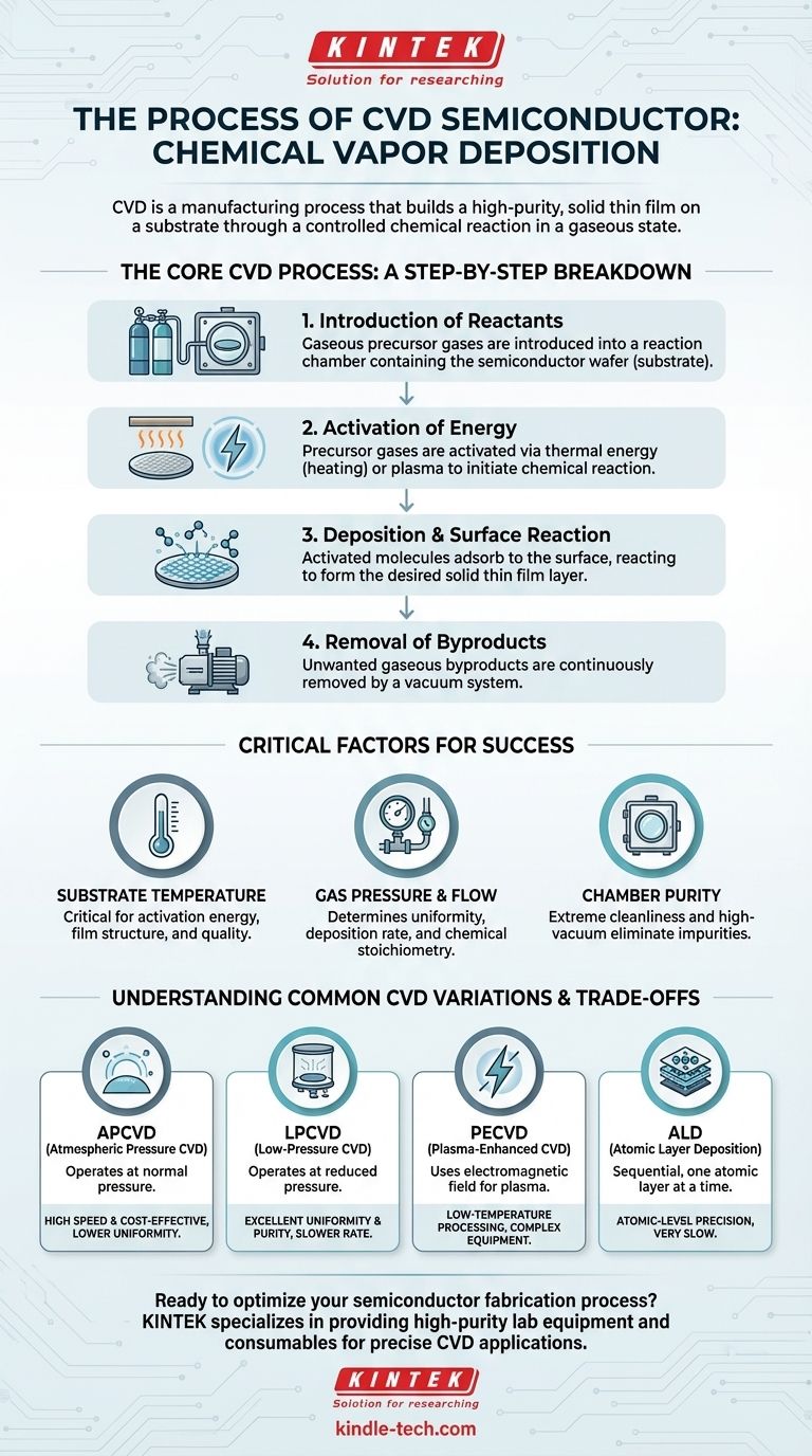
The Core CVD Process: A Step-by-Step Breakdown
The entire process, from gas injection to film formation, can be understood as a sequence of four critical stages. Each stage is precisely controlled to determine the final properties of the deposited film.
Step 1: Introduction of Reactants
The process begins by introducing two or more gaseous raw materials, called precursor gases, into a reaction chamber containing the semiconductor wafer (the substrate).
The purity of these gases and the cleanliness of the chamber are paramount, as even minuscule impurities can compromise the electrical properties of the final device.
Step 2: Activation of Energy
The precursor gases are stable at room temperature and must be "activated" with energy to initiate a chemical reaction.
This activation is typically achieved through thermal energy, by heating the substrate to hundreds or even thousands of degrees Celsius. Alternatively, methods like plasma can be used to energize the gases at much lower temperatures.
Step 3: Deposition and Surface Reaction
Once activated, the gas molecules diffuse through the chamber and adsorb (form a bond with) the substrate's surface.
This is where the key chemical reaction occurs. The adsorbed molecules react to form the desired solid film, permanently bonding to the wafer. The structure and quality of this film depend heavily on the conditions in the chamber.
Step 4: Removal of Byproducts
The chemical reaction that forms the solid film also produces unwanted gaseous byproducts.
These byproducts are continuously removed from the chamber by a vacuum system. Efficient removal is essential to prevent them from interfering with the deposition process or getting incorporated into the film as contaminants.
Critical Factors for a Successful Deposition
The success of the CVD process hinges on the meticulous control of several environmental variables. These factors directly influence the thickness, uniformity, and chemical composition of the deposited layer.
Substrate Temperature
Temperature is arguably the most critical variable. It not only provides the activation energy for the chemical reaction but also influences the mobility of atoms on the surface, which affects the film's crystalline structure and quality.
Gas Pressure and Flow
The pressure inside the reaction chamber determines the path and concentration of the precursor gas molecules. Lower pressures lead to better film uniformity, while atmospheric pressure allows for faster deposition rates. The flow rates of each gas control the chemical stoichiometry of the reaction.
Chamber Purity
Semiconductor fabrication demands extreme cleanliness. The process is performed in a high-vacuum environment to eliminate oxygen, moisture, and other reactive particles. Any residual gas is purged to ensure that only the intended chemical reaction occurs.
Understanding the Trade-offs: Common CVD Variations
No single CVD method is perfect for all applications. Engineers choose a specific technique based on the required film properties, temperature constraints, and manufacturing costs.
APCVD (Atmospheric Pressure CVD)
This method operates at normal atmospheric pressure. It is characterized by very high deposition rates, making it fast and cost-effective. However, the film quality and uniformity can be lower than other methods.
LPCVD (Low-Pressure CVD)
By operating at a reduced pressure, LPCVD significantly improves film uniformity and purity. The lower pressure reduces unwanted gas-phase reactions, ensuring the chemistry happens primarily on the wafer surface. The main trade-off is a slower deposition rate.
PECVD (Plasma-Enhanced CVD)
PECVD uses an electromagnetic field to create plasma, which energizes the precursor gases. This allows deposition to occur at much lower temperatures (e.g., < 400°C), which is crucial for protecting sensitive device structures already built on the wafer.
ALD (Atomic Layer Deposition)
ALD is an advanced, sequential form of CVD where precursor gases are introduced one at a time. This process deposits a perfectly uniform film exactly one atomic layer at a time. It offers unparalleled control and conformity over complex 3D structures but is significantly slower than other methods.
Matching the CVD Method to Your Goal
The choice of CVD technique is always a strategic decision driven by the end goal for the specific layer being deposited.
- If your primary focus is high throughput for thick, less-critical films: APCVD offers the speed and cost-efficiency required for such applications.
- If your primary focus is high purity and uniformity for critical layers like polysilicon: LPCVD is the industry standard for producing high-quality, repeatable films.
- If your primary focus is depositing a film without damaging underlying layers: PECVD is essential when the fabrication process is constrained by a strict thermal budget.
- If your primary focus is ultimate precision and coating complex 3D nanostructures: ALD is the only technique that provides the atomic-level control necessary for modern, cutting-edge devices.
Ultimately, Chemical Vapor Deposition is the foundational technology that enables engineers to build the complex, multi-layered structures that define every modern microchip.
Summary Table:
| CVD Method | Primary Advantage | Key Limitation | Ideal Use Case |
|---|---|---|---|
| APCVD | High deposition rate, cost-effective | Lower film uniformity | Thick, less-critical films |
| LPCVD | Excellent uniformity and purity | Slower deposition rate | Critical layers like polysilicon |
| PECVD | Low-temperature processing | More complex equipment | Temperature-sensitive structures |
| ALD | Atomic-level precision, perfect conformity | Very slow deposition | Complex 3D nanostructures |
Ready to optimize your semiconductor fabrication process? KINTEK specializes in providing high-purity lab equipment and consumables for precise CVD applications. Whether you need reactors, precursor delivery systems, or vacuum components, our solutions ensure the extreme cleanliness and control required for successful thin film deposition. Contact our experts today to discuss how we can support your laboratory's semiconductor manufacturing needs.
Visual Guide
Related Products
- Chemical Vapor Deposition CVD Equipment System Chamber Slide PECVD Tube Furnace with Liquid Gasifier PECVD Machine
- Customer Made Versatile CVD Tube Furnace Chemical Vapor Deposition Chamber System Equipment
- HFCVD Machine System Equipment for Drawing Die Nano-Diamond Coating
- Split Chamber CVD Tube Furnace with Vacuum Station Chemical Vapor Deposition System Equipment Machine
- Multi Heating Zones CVD Tube Furnace Machine Chemical Vapor Deposition Chamber System Equipment
People Also Ask
- What types of substrates are used in CVD to facilitate graphene films? Optimize Graphene Growth with the Right Catalyst
- What happens during deposition chemistry? Building Thin Films from Gaseous Precursors
- How expensive is chemical vapor deposition? Understanding the True Cost of High-Performance Coating
- What is the chemical vapor deposition growth process? Build Superior Thin Films from the Atom Up
- What are the core advantages of PE-CVD in OLED encapsulation? Protect Sensitive Layers with Low-Temp Film Deposition


