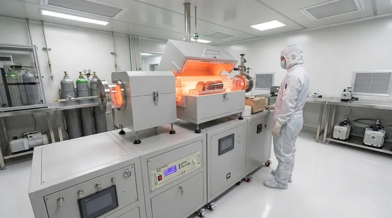
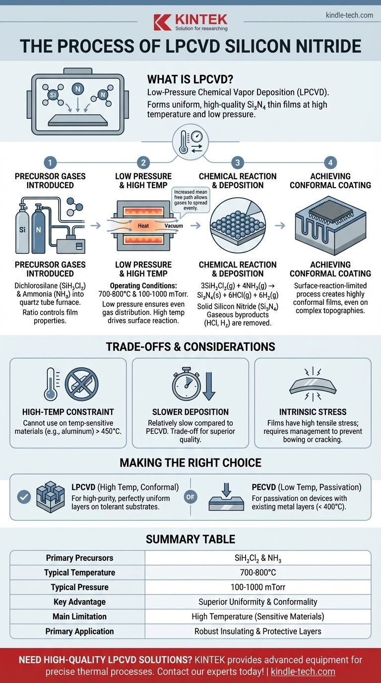
To be precise, Low-Pressure Chemical Vapor Deposition (LPCVD) of silicon nitride is a process where a silicon-containing gas and a nitrogen-containing gas react at high temperatures and low pressure inside a chamber. This controlled chemical reaction forms a solid, highly uniform thin film of silicon nitride (Si₃N₄) directly onto a substrate, such as a silicon wafer. It is a cornerstone technique in microfabrication for creating robust insulating and protective layers.
The central principle of LPCVD is using high temperature to drive a surface chemical reaction and low pressure to ensure the reactant gases can spread out evenly. This combination produces exceptionally uniform and pure silicon nitride films that can conform to complex surface topologies, but it cannot be used on temperature-sensitive materials.
The Fundamental LPCVD Process
LPCVD for silicon nitride is not a single action but a sequence of carefully controlled steps. The quality of the final film depends on precise control over each stage of this thermal and chemical process.
The Introduction of Precursor Gases
The process begins by introducing two primary precursor gases into a high-temperature quartz tube furnace.
The most common precursors are dichlorosilane (SiH₂Cl₂) as the silicon source and ammonia (NH₃) as the nitrogen source. Their ratio is carefully controlled to determine the final film's properties.
The Role of Low Pressure and High Temperature
The defining characteristics of the process are its operating conditions. The furnace is held at a low pressure (typically 100-1000 mTorr) and a high temperature (typically 700-800°C).
Low pressure increases the mean free path of the gas molecules, allowing them to travel farther without colliding. This ensures that the precursor gases distribute evenly throughout the chamber and across all substrate surfaces before reacting.
High temperature provides the thermal energy necessary to initiate the chemical reaction on the substrate surface.
The Chemical Reaction on the Substrate
Once the precursor gases reach the heated substrate, they have enough energy to react and decompose, forming a solid film. The simplified overall chemical reaction is:
3SiH₂Cl₂(g) + 4NH₃(g) → Si₃N₄(s) + 6HCl(g) + 6H₂(g)
The solid silicon nitride (Si₃N₄) deposits on the substrate surface, while the gaseous byproducts, hydrogen chloride (HCl) and hydrogen (H₂), are removed from the chamber by the vacuum system.
Achieving a Conformal Coating
Because the reaction is primarily driven by the high surface temperature and not limited by how fast the gas arrives, it is known as a surface-reaction-limited process.
This is the key to LPCVD's most significant advantage: creating highly conformal films. The film deposits at a uniform rate on all surfaces, including vertical sidewalls and deep trenches, which is critical for fabricating complex, three-dimensional microelectronic devices.
Understanding the Trade-offs
While powerful, the LPCVD process involves critical trade-offs that dictate where it can and cannot be used in a manufacturing flow.
The High-Temperature Constraint
The most significant limitation of LPCVD silicon nitride is its high deposition temperature.
Temperatures above 450°C can melt or damage certain materials, most notably aluminum, which is commonly used for electrical interconnects. This means LPCVD silicon nitride cannot be deposited after such metals have been placed on the wafer.
Slower Deposition Rates
Compared to alternative methods like Plasma-Enhanced CVD (PECVD), the deposition rate for LPCVD is relatively slow. This is a direct trade-off for achieving superior film quality and uniformity.
Intrinsic Film Stress
LPCVD silicon nitride films naturally form with high tensile stress. If not properly managed by adjusting deposition parameters, this stress can cause the wafer to bow or even lead to film delamination and cracking, compromising device integrity.
Making the Right Choice for Your Goal
Selecting a deposition method requires a clear understanding of your device requirements, particularly thermal budget and the need for conformality.
- If your primary focus is creating a high-purity, perfectly uniform insulating layer on a temperature-tolerant substrate: LPCVD is the definitive choice due to its superior conformality and film quality.
- If your primary focus is depositing a passivation layer on a device with existing metal layers: Plasma-Enhanced CVD (PECVD) is the necessary alternative, as it operates at much lower temperatures (typically < 400°C), protecting the sensitive components.
Ultimately, understanding the interplay between temperature, pressure, and film properties is the key to leveraging the right deposition technique for your specific application.
Summary Table:
| LPCVD Silicon Nitride Process | Key Details |
|---|---|
| Primary Precursors | Dichlorosilane (SiH₂Cl₂) & Ammonia (NH₃) |
| Typical Temperature | 700-800°C |
| Typical Pressure | 100-1000 mTorr |
| Key Advantage | Superior uniformity & conformality on complex surfaces |
| Main Limitation | High temperature restricts use on sensitive materials |
| Primary Application | Robust insulating & protective layers in microelectronics |
Need a high-quality, uniform silicon nitride film for your microfabrication process?
At KINTEK, we specialize in providing advanced lab equipment and consumables for precise thermal processes like LPCVD. Our expertise ensures you achieve the conformal coatings and superior film quality your R&D or production demands.
Let's discuss your specific application requirements. Contact our experts today to find the perfect solution for your laboratory needs!
Visual Guide
Related Products
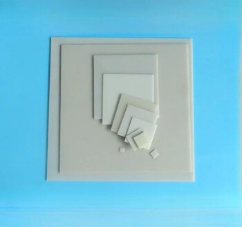
- Precision Machined Silicon Nitride (SiN) Ceramic Sheet for Engineering Advanced Fine Ceramics
- Inclined Rotary Plasma Enhanced Chemical Vapor Deposition PECVD Equipment Tube Furnace Machine
- Inclined Rotary Plasma Enhanced Chemical Vapor Deposition PECVD Equipment Tube Furnace Machine
- Chemical Vapor Deposition CVD Equipment System Chamber Slide PECVD Tube Furnace with Liquid Gasifier PECVD Machine
- Advanced Engineering Fine Ceramics Aluminum Nitride (AlN) Ceramic Sheet
People Also Ask
- Which is the most preferred material for manufacturing of a semiconductor? Silicon's Dominance Explained
- What are the methods of high temperature ceramic? Master the 3-Stage Process for Durable Components
- What is sintered ceramic? A Durable, Non-Porous Material for Modern Surfaces
- What is the most commonly used in semiconductors? Discover Why Silicon Dominates Modern Electronics
- What is the sputtering target of gallium oxide? A Guide to High-Performance Ga₂O₃ Thin Films